6
\$\begingroup\$

When using an optocoupler, is there a difference performance'wise whether using a collector or an emitter resistor?

When using a normal transistor the base to emitter voltage gain is approximately 1, whereas base to collector gain is much larger. With an optocoupler however, base is not (necessarily) at a definded absolute voltage. For this question I am disregarding optocouplers that have the base available on one of the pins, or at least having an external bias.

So apart from inverting properties, are these identical (R1, Q1 vs. R2, Q2) or is there a difference (eg. in frequency response [parasitic capacity], different rise/fall times, gain, ...). And when using both collector and emitter resistors (R3C, R3E, Q3), will the signal be symmetric or should I account for base current like in a regular BJT circuit (as in \$\frac{\beta}{\beta+1} = \frac{I_C}{I_E}\$). In other words, where does the base current go in this closed circuit?
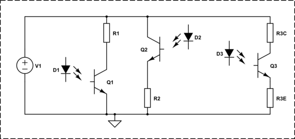
schematic

simulate this circuit – Schematic created using CircuitLab

\$\endgroup\$
2
  • 1
    \$\begingroup\$ That's an interesting question. About your last point, I do not see any way for which base current can be different from zero. Usually base current is present because the charge in the base region must be sustained since there are some losses, here the charge is photogenerated so no current flows into base, collector and emitter currents are exactly the same. \$\endgroup\$ Commented Mar 6, 2016 at 11:20
  • 1
    \$\begingroup\$ @VladimirCravero that is exactly what I'm trying to figure out. Maybe the question behind this is how a photo-transistor works with regard to assumed (photo) base current. \$\endgroup\$
    – jippie
    Commented Mar 6, 2016 at 11:41

3 Answers 3

3
\$\begingroup\$

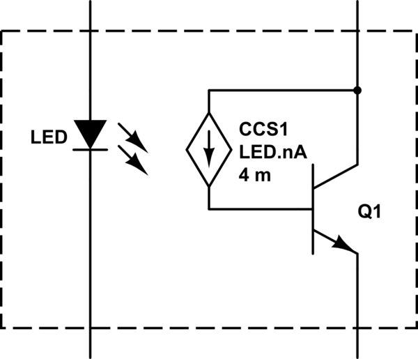
where does the base current go in this closed circuit?

Photoelectric current current flows from the Collector to the Base. If the Base is left open then it also flows into the Emitter, so Collector and Emitter currents are identical. The equivalent circuit looks like this:-

schematic

simulate this circuit – Schematic created using CircuitLab
\$\endgroup\$
5
\$\begingroup\$

They are two terminal devices so the performance is mirrored for common emitter vs. common collector configuration.

Common emitter has slow rise time and fast fall time. Common collector has fast rise time and slow fall time.

\$\endgroup\$
4
  • 1
    \$\begingroup\$ I had to read this three times to get it. You're saying that because photo-transistors turn off more slowly than they turn on that the R-Q junction of the common emitter will rise more slowly than it falls. Vice-versa for the common collector circuit. Have I got it? \$\endgroup\$
    – Transistor
    Commented Mar 6, 2016 at 19:16
  • \$\begingroup\$ Yes, exactly .. \$\endgroup\$ Commented Mar 6, 2016 at 20:15
  • \$\begingroup\$ Is this a symmetric effect? E.g. looking at the maximum switching frequency, is it strictly identical in both configurations? \$\endgroup\$
    – ARF
    Commented May 15, 2016 at 23:37
  • 1
    \$\begingroup\$ It should be very close- especially for a shielded optocoupler. There might be a slight effect due to coupling through the LED in non-shielded types. \$\endgroup\$ Commented May 15, 2016 at 23:55
5
\$\begingroup\$

Excellent question - I remember struggling with this a while ago.

For a phototransistor, the key parameter is the current transfer ratio which is analogous to hfe (and shares many key parameters, such as variation vs. If).

The CTR is after all, I(out) / I(in).

In general, a phototransistor can be viewed as a photodiode where the output current is fed to the base of an ordinary transistor.

I most definitely agree that there is no current into or out of the base in the normal sense for the device as drawn.

In the above cases, add a current source on the bases of the transistors where the current is proportional to incident energy and you will have quite an accurate representation of what is going on.

schematic

simulate this circuit – Schematic created using CircuitLab
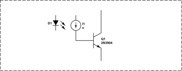
Here is the representation I normally use.

The base emitter biasing is generated by incident light generating electron hole pairs which diffuse into the silicon; the light needs to be of sufficient energy, of course.

Where does that current go? When the minority carriers reach the junction, they are swept across by the electric field set up from Collector Emitter bias.

The device acts as a (poor grade) current source, just as an ordinary bipolar device does, and there is an excellent description of just what is going on available.

For the above reasons, you can analyse a phototransistor just the same as a bipolar device provided you take into account the different parameters; a limitation is that you need to use currents (as you note, there is no specific voltage associated with the base).

Note: When looking at this sort of thing, I view it as an energy transfer function as that makes things a bit clearer - i.e. some energy went in and therefore that energy must appear somewhere else.

\$\endgroup\$

Your Answer

By clicking “Post Your Answer”, you agree to our terms of service and acknowledge you have read our privacy policy.

Not the answer you're looking for? Browse other questions tagged or ask your own question.