3
\$\begingroup\$

As I'm reading about switch-mode power supplies (SMPS) I keep coming across the term clamped inductive load.

You'd think there would be a clear definition that would pop up as the first Google hit, but no such luck (for me anyway :).

What exactly is a clamped inductive load? And in particular what is being clamped? and what is doing the clamping?

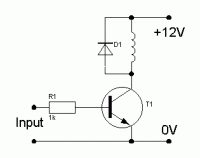
I get that something like this probably counts as one:

enter image description here

.. but I have only the vaguest idea what makes it so.

It seems to be something that crops up over and over in an SMPS context (re:switching MOSFETs, snubbers, etc.), so I'd like to have a clear idea how to distinguish one and what makes it important :)

\$\endgroup\$

3 Answers 3

5
\$\begingroup\$

You have a clamped inductive load and what is known as the inductive kickback voltage is what is being clamped.

Consider the current in the inductor with the transistor on at some time \$t_0\$ with a current \$I_0\$.

Now turn the transistor off, remembering it will not be instantaneous. The current will go from \$I_0\$ to zero in some time \$t_x\$.

As the current is decreasing, we have a change in current of \$ -\frac {\delta I} {\delta t}\$ (which is really more accurate in this case assuming a linear rate of change of current).

Merging our current against the standard equation for inductive kick, the voltage across this inductor is therefore \$ (-)(-)\ L\frac {\delta I} {\delta t}\$; this is an important point - the voltage at the collector of the transistor (if not clamped) can reach enormous potentials.

If I take a load current of a modest 50mA and a switching time of 20 nsec (not at all uncommon), with an inductor of 20μH then the collector voltage would go to 62V, given by the inductive kick plus the 12V supply (and probably more as the true instantaneous rate of change may well be faster at some point during the current decay).

This would destroy a 40V part; the diode clamps the collector at no more than Vcc + a diode drop (about 12.7V) and forms a circulating current loop for the decay current when the switch is turned off.

It can be informative to see the test circuit for an unclamped inductive load (often specified for MOSFETS):

MOSFET unclamped inductive load test

Here, a clamping action is achieved by the internal avalanche diode inherent within the MOSFET.

\$\endgroup\$
1
  • \$\begingroup\$ Thanks Peter, that's just the definition I was looking for :) I understood the dynamics of the circuit ok, it was just the term I was fuzzy on. The comparison with unclamped goes a long way to clarify. Some of my uncertainty was coming from the fact that in an SMPS, the current through the diode is generally the useful product of the circuit rather than parasitic energy to be dissipated. Your explanation also helps me understand that other mechanisms could be used to do the clamping, like perhaps a zener or a carefully-timed secondary MOSFET. \$\endgroup\$
    – scanny
    Commented Jun 28, 2016 at 17:52
6
\$\begingroup\$

Let's imagine your example circuit, except with the inductor replaced with a resistor. This is a really simple circuit: when the transistor is on, the current through it is given by V = IR. When the transistor is off, no current flows.

Now, add the inductor back in. The inductor does not like the current flowing through it to change: however many amps it is (0, 1, or 42), the inductor wants it to stay like that (due to storing energy as a magnetic field: you have to 'charge up' the magnetic field to increase current or 'discharge'it to reduce current). It resists complying with V = IR.

So, in the example circuit, when the transistor is turned on, it will take a while for the current to ramp up to its full value. In most cases, you don't really care. The problem comes when you turn off the transistor: the inductor doesn't want the current flow to stop, and keeps ramming charge through itself at the transistor. The energy stored in the magnetic field in the inductor has got to go somewhere. This causes a HUGE voltage spike between the inductor and the transistor that is likely to exceed the voltage rating of the transistor and damage it.

That is what the clamping diode is there to prevent: it will prevent that node between the inductor and the transistor from rising above the voltage of the power supply and damaging your transistor.

\$\endgroup\$
1
\$\begingroup\$

The transistor T1 causes current to flow from the +12 VDC source and through the inductor. The current will eventually level off at some point due to the DC resistance of the inductor.

If the current in the base of T1 is decreased, T1 stops the current flow in the inductor as well. At this point the magnetic field collapses, which can result in the voltage across the coil "reversing". That is to say current would try and flow in the opposite direction. The diode D1 becomes forward biased and appears as a very low impedance circuit for the current in the inductor. In this way, D1 "clamps" the inductor.

\$\endgroup\$
1
  • 3
    \$\begingroup\$ While \$v_L\$ may reverse its polarity when the switch turns off, it does not follow that \$i_L\$ will reverse direction. What would reverse in that case is \$\frac{di_L}{dt}\$, meaning the current would stop increasing and start decreasing. \$\endgroup\$
    – scanny
    Commented Jun 28, 2016 at 4:03

Your Answer

By clicking “Post Your Answer”, you agree to our terms of service and acknowledge you have read our privacy policy.

Not the answer you're looking for? Browse other questions tagged or ask your own question.