To understand your own question and to answer it yourself and to understand other answers you need to understand what you are measuring, what you are trying not to measure and how various factors affect these. Overall that is too large a subject to be answered briefly, but the following (not especially brief :-) ) notes should provide enough outline to guide your understanding of the large amount of material available online.
This question and the TI reference Three guidelines for designing anti-aliasing filters are couched in terms of anti aliasing filters, but the issue is broader. An antialisasing filter is used to remove signals at frequencies above the ADC's "Nyquist limit" so that they are not converted into apparent in-band signals by 'aaliasing'. However, addition of filters (CM especially) can increase the amount of in band or apparent in band signal if "done wrong".
Application: Use of a dual input "differential" ADC to
I'll refer to these as OOB signal or CM OOB or DM OOB as appropriate.
CM signal is a tautology as CM signal is "OOB" at any frequency - wherever it is, you don't want it. In an ideal case it is also irrelevant, and such filters as are needed are to account for non idealities in the system.
You can also have in-band differential noise, which is outside the scope of this discussion. You can also have DM OOB below the signal frequency but as this discussion is biased towards anti-aliasing filters I'll not consider low frequency DM OOB.
So ...
Vcm - common mode voltage
Vdiff - differential input voltage
The ideal situation is to have an
The ideal differential converter is immune to CM noise (by definition).
ie An ideal DM converter happily rejects any degree of CM OOB so is CM OOB immune so needs no CM OOB filter.
There are two cases (at least) of non ideality that make a CM filter needed.
An ADC has a CM Vin range spec which is usually at best equal to the power supply range (0V to Vdd for single supply ADC, +/- Vdd for dual supply) and is often somewhat less than Vdd on the high side. A dual supply ADC may have Vcm limited to less than +/- Vdd on both rails but single supply ADCs usuall allow Vin=ground.
So, to meet this requirement Vin_CM must be less than the allowable Vcm range. This is usually an extremely easy spec to meet - eg any time you have more than eg +/- 5 VAC CM noise on the patient you may wish to redesign your system. In some non-medical systems very high Vcm may exist and a filter may be needed.
Harder is when a non differential amplifier is used. It is "common enough" for a "differentiaal" ADC to in fact use two separate independent channels and for the differential signal to be derived as the difference between channels. Any difference in response to CM signal or any difference in gain or frequency response to CM will show up as apparent Vdiff. If Fcm is in the frequency band this will appear as apparent true diff. If this is above the frequency band it will appear as aliased apparent true Vdiff.
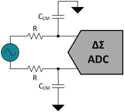
As a bonus, adding CM filtering CAN make matters worse. If the filtering is unbalanced then a perfectly balanced CM signal which is not causing problems may be converted to a differering input level on each signal lead and introduce errors. In the reference you provided their Figure 2 is shown below. If the two R's are non identical or the two C's are non identical then the equal (by definition) CM input signal will be converted to a differential difference at the ADC input.

Summary: So, the amount of CM OOB filtering that is needed is what is required to meet all the above requirements to such an extent that the remaining apparent true Vdiff caused by Vcm is << 1 ADC LSB.
The basic IC Vcm spec is not usually exceeded by the input signal and a filter that gets this into range is "easy". The reduction to meet ADC imbalance (due to input line errors such as capacitor mismatch) is more subtle and you need to do some calculations based on maximum expected Vcm and component tolerances and values.
The excessively enthused may wish to look at ADC input impedance and possible variations in channel parameters - these should be able to be discounted as they are usually easily swamped by external component magnitudes (and should be). (A data sheet may specify worst case variation in eg input capacitance but usually does not look at differential variations which are liable to be small on the same IC).
Having spent so much time on Vcm, the Vdm portion will be (relatively) mercifully brief.
With an ideal true differential ADC DM OOB signal should be small enough that aliased components are << 1 ADC LSB.
DM OOB can be sourced from the input system and "generated by" CM signal interacting with imbalanced CM filters, as above. In the case of true input DM OOB the magnitude should be able to be calculated from known sources (or measured if required) and a filter provided which reduces the worst case level as required. For DM OOB converted from badly handled CM OOB the first step is "design so as to not let it happen" and the second is to add enough DM filtering to allow for the worst case of converted signal.
It is arguably easier to filter converted CM signal that appears as above frequency DM signal than to prevent the conversion. Thi is because imbalance in the CM filter depends on component matching and while 0.1% tolerance resistors are low cost and readily available, 1% capacitors are the normal common limit and 0.1% capacitors are probably only available using SOT ("select on test") and liable to not achieve that accuracy across temperature and time. Whereas ...
A DM antialisaing filter may be made "arbitrarily good" by increasing its out of band (high frequency) rejaction as required. This can be achieved with a simple ilter (eg 1 pole passive) far enough below the Nyquist frequency, or by a multipole filter closer to the desired cutoff freqeuency.
Where the ADC has a conversion rate (sampling period) substantially higher than the maximum signal frequency a simple filter will suffice.
Alas, in the real world conversion rate and available bits compete and eg Delta Sigma converters with very high available bits of conversion resolution also have low sampling rates.
SO overall - all factors need to be considered and an solution used that meets known inband and worst case OOB levels converter characteristics, component tolerances (and Murphy).

