0
\$\begingroup\$

Following up interesting discussion here with John Birckhead (@JohnBirckhead), I decided to ask separate question on the issue.

Here's my circuit

enter image description here

The circuit includes UDA1334BTS, DAC powered from +3.3 V, connected using its typical application diagram (see page 16, fig. 8) and AD8512 op-amp, powered from ±12 V. Initially we were troubleshooting the problem of my circuit not working with two new op-amp chips, with chips looking like defective or damaged.

John proposed that while circuit looks good, there's a problem when it is being turned off.

Capacitors C66 and C57, which are of 47 uF value, discharge too slowly through DAC output and 220k resistors of respective channel; when system is turned off, ±12 V supply is removed very quickly, but potential capacitors are charged to remains for next several seconds, violating condition explained in datasheet that

[AD8512] have internal protective circuitry that allows voltages as high as 0.7 V beyond the supplies to be applied at the input of either terminal without causing damage.

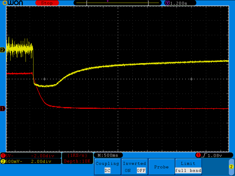
Let's look what is going on in my circuit:

enter image description here

We can clearly see that power goes off exponentially (red), at the same time op-amp's input is about -1.2 V.

However further datasheet states that

For higher input voltages, a series resistor is necessary to limit the input current. The resistor value can be determined from the formula (Vin - Vs)/Rs ≤ 5 mA.

I am confused here - what matters - over-voltage, or over-current? In my circuit there's series resistor of 100 Ohm, when power if completely gone current flowing through resistor (approximately) ( -1.2 V - 0 ) / 100 = 12 mA, higher than required by datasheet.

John has proposed putting negative voltage limiting diodes (manually drawn connections on the circuit diagram), these diodes would make caps discharging faster.

I want to know your opinion - is there any other way to mitigate this effect? I think I did not see many circuit diagrams having diodes before op-amps.

Probably it is a matter of tuning DAC's typical application circuit, C66 and C57 values (e.g. from 47 uF down to 1 uF), decreasing values of R29 to R44 (e.g. from 220k to 10k), and increasing value of series resistor (e.g. from 100 Ohm to 220 Ohm)?

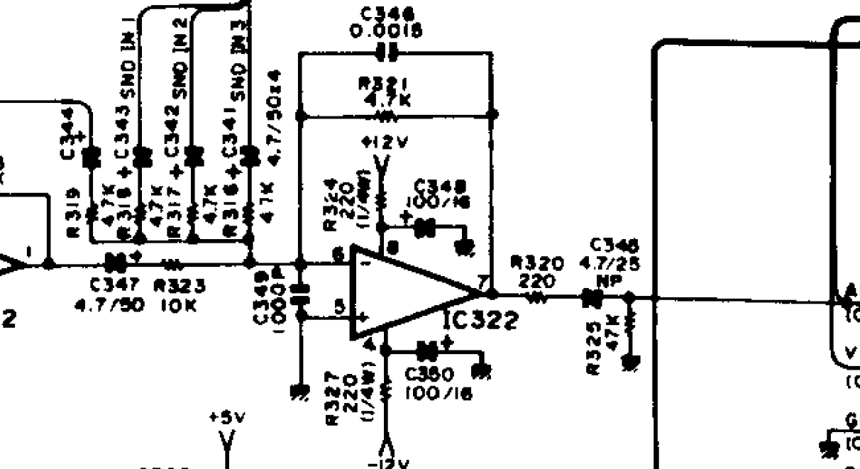
As a side note, I have old computer with mixer (NJM4558-based)

enter image description here

and it also exhibits these issues when powering on or off, but, as far as I can see, voltage on its op-amp input goes down relatively the same rate as power voltage. In my case input voltage is too long outside of allowed range relative to power.

\$\endgroup\$

2 Answers 2

1
\$\begingroup\$

The diodes as shown are going to cause some distortion at higher signal levels.

You can meet the input current limit requirements by changing the resistors R45/R28 to 1K and decreasing C67/C58 to 1000pF. That maintains the same RC time constant and limits the worst case current (which is 3.3V/1K) to less than 5mA.

If you do add diodes, they should be to the supplies of the op-amp not to ground. For example, you could use a BAT54S and connect it to the input and to the +/-12V supplies. It's not necessary in this case, however.

\$\endgroup\$
2
  • \$\begingroup\$ I am slightly hesitant adding diodes this way, if one of them fail in the field I may get into big trouble. DAC outputs voltage of 0-3.3 V (always positive), thus 1k must be enough to keep 3.3 mA internal clamping current. Would you agree? Should I also change 220k resistor value (and by the way, why it is there, and why 220k?) \$\endgroup\$
    – Anonymous
    Commented Jun 15, 2017 at 15:04
  • 1
    \$\begingroup\$ Yes, you are correct. The 220K/47uF controls how fast the op-amp input approaches 0V when powered up- the average DAC output is Vdda/2. It is a high-pass filter with a sub-1Hz rolloff. If your entire amplifier was DC coupled and had no power-up mute the speaker cones would slam over to one side and then slowly return. You don't need to change them as a result of changing the other parts. Diodes failing in the field should not be a big worry- they can handle 600mA surge 200mA continuous and 30V, none of which should exist in your circuit. \$\endgroup\$ Commented Jun 15, 2017 at 15:16
2
\$\begingroup\$

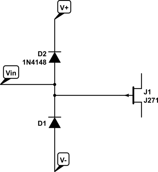
The input stage (for each input) will look something like this:

schematic

simulate this circuit – Schematic created using CircuitLab

D1 and D2 are clamping diodes, and cannot handle more than 5mA continuous (a fairly typical situation), so what matters is self-heating in these diodes. These are standard silicon diodes in this instance (the 0.7V rating gives it away).

This is sometimes listed as the maximum pin injection current, incidentally.

It really is not at all unusual to see external clamp diodes (use Schottky devices) on input to prevent the amplifier input voltages achieving a voltage so that the internal clamps do not turn on when it is not practical to use series resistors.

\$\endgroup\$
2
  • \$\begingroup\$ Thank you. I found this article analog.com/en/analog-dialogue/articles/…, it has resistor before clamping circuit, and same value resistor in feedback to negative input (as I understand to keep gain 1). In my case would it be appropriate to just increase value of series resistor to 1k so that internal clamping current would be max 3.3/1000=3.3 mA, within specifications, and include resistor of some value to keep gain at specific level (output voltage range)? \$\endgroup\$
    – Anonymous
    Commented Jun 15, 2017 at 14:59
  • 1
    \$\begingroup\$ You could indeed use that method. Note that the resistor in the feedback loop is to balance any offsets due to the inputs seeing a different source impedance, but as the input to this device is a JFET, I would consider it optional here. \$\endgroup\$ Commented Jun 15, 2017 at 15:08

Your Answer

By clicking “Post Your Answer”, you agree to our terms of service and acknowledge you have read our privacy policy.

Not the answer you're looking for? Browse other questions tagged or ask your own question.