simulate this circuit – Schematic created using CircuitLab
I came up with this circuit myself and have neither simulated nor built it, so I very highly recommend you take this as a "concept" rather than a fully built circuit. The parts are arbitrarily picked (treat the 2N3904 simply as an arbitrary NPN etc.). As I don't know what kinds of transistors you're using I just used an NPN for your driving transistor.
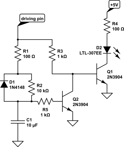
D2, R4, Q1, and R3 are all parts that I assumed are in your circuit. The remaining parts make up the circuit I've added.
Let us assume the driving pin is high:
The circuit begins with C1 initially at 0 volts, charging through R1 and R2. As the voltage over Q2's base-emitter section is well below it's threshold to sink any current through the collector, nearly no current is drawn. The circuit behaves as if nothing is happening and acts as you originally intended. As C1 charges through R1 and R2, Q2 begins to turn on a little bit and the voltage at Q1's base drops a small amount as Q2's collector begins pulling more current. As C1 charges further, eventually Q2 is on enough so that the voltage at Q1's base isn't enough to drive the transistor to drive the LED (around 0.6 volts or so probably), and thus Q1 is turned off after a delay.
When the driving pin goes low, the capacitor will discharge quickly through R1, much faster than it does through R2 and R1, resetting the circuit in about 100th of the time as it takes to be set in the first place (100 being roughly the ratio between R1 and R2).
Again, the values I've picked are arbitrary so you will likely have to experiment with R1 and R2 values until you find a delay that works for you. R1 I would say should always be 100 ohms or greater to protect the driving pin being damaged when the capacitor discharges. The R2:R1 ratio should be kept large to allow for fast discharge times, keep R2 at least 10 times greater than R1 I would say. C1 can be basically any value you want, but you'll probably end up with something around 1 microfarad. Q2 needs to be an NPN for this to work in it's current form, however the concept should be convertible to a form that uses any transistors you happen to be using. Q1 just needs to be a transistor that turns the LED on when the base is at a high voltage relative to it's grounded side (which I assumed was how your circuit works).
The time this circuit takes until it "activates" is dependant on R1, R2, and C1. Assuming the circuit activates once C1 has charged to about 1 volt and the driving pin uses 5V logic, I would estimate the time to activate would be (R1 + R2)*C1/5 or so. This a quick estimate based on the fact that the time it takes for the capacitor to charge up about 2/3 of the way is (R1 + R2)*C1.
Again, don't take this circuit for gospel as I have put this together very quickly. I recommend making your own version simply based on these ideas and then simulating and building it.
EDIT: As pipe pointed out, my value for R3 is too small, as it will allow ~5mA to flow while the LED is off. Replacing it with a larger value (20K or so) would make the circuit work with much less current draw. Increasing this value too high will prevent Q1 from being able to turn on at all, you will probably start having problems around 100K (another rough estimate).


