3
\$\begingroup\$

LOW side MOSFET turn on

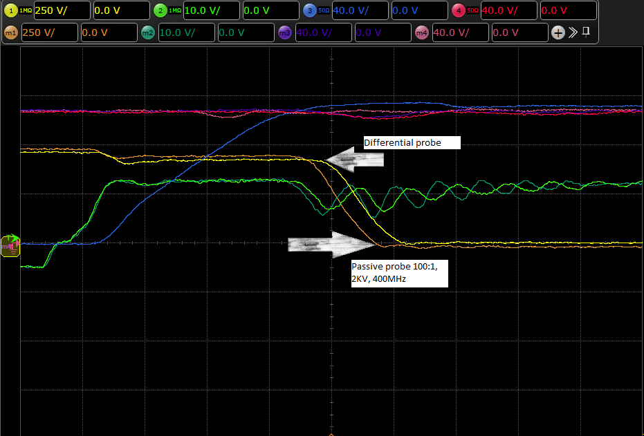
In the image:

  • Channel 1: Drain to source voltage
  • Channel 2: gate to source voltage
  • Channel 3: Switch current
  • Channel 4: Load current

The image shows Vds of low side MOSFET at turn on measured with a passive and differential probe separately. As you can see, differential probe has a skew compared to passive probe, which is understandable.

But: Why does the reading, after turning on the passive probe, become negative whereas the differential probe still shows the correct reading?

\$\endgroup\$
5
  • \$\begingroup\$ How did you adjust the vertical position in the first place? If you used the active probe, and it had a DC offset, the passive probe would appear to have the opposite DC offset (unless you readjusted). Also, the passive appears to have higher gain and we're looking at a short timescale. So ... did you remember to calibrate the passive probe first? \$\endgroup\$
    – user16324
    Commented Jan 9, 2018 at 13:35
  • \$\begingroup\$ @ Brian Drummond i have not done any vertical scaling. The differential probe I used is pico TA058. So can you explain what do u mean by a DC offset. and I did not calibrate the passive probe first. It was already being used in lab by others, So i thought, it must have been calibrated \$\endgroup\$
    – Autobot
    Commented Jan 9, 2018 at 13:50
  • 2
    \$\begingroup\$ @Autobot : "I did not calibrate the passive probe first. It was already being used in lab by others" this is bad behavior, recalibrate when you start your tests (and write about it in your report) as a lab manager, i've seen day's worth of work thrashed because of that behavior \$\endgroup\$
    – Sclrx
    Commented Jan 9, 2018 at 13:55
  • 1
    \$\begingroup\$ @Sclrx I checked the calibration again and it was fine. \$\endgroup\$
    – Autobot
    Commented Jan 9, 2018 at 15:08
  • \$\begingroup\$ @Brian Drummond My differential probe does have a positive offset but just of 55mV, so i guess that doesn't explain much higher negative offset in my passive probe \$\endgroup\$
    – Autobot
    Commented Jan 11, 2018 at 10:18

1 Answer 1

0
\$\begingroup\$

It's probably an effect of parasitic impedance in the passive probe system that doesn't show up for the higher-performing differential probe. It's a pretty minimal negative value, so I wouldn't read too much into it. I'm sure if you give our support center a call an AE would be happy to talk with you in more detail.

\$\endgroup\$
4
  • \$\begingroup\$ What do you exactly mean by higher performing? CMRR? My differential probe is 50 MHz and passive probe is 400 MHz. In this experiment, I am calculating energy losses, and differential probe being of lower bandwidth attenuates my high frequency components, and giving me slower waveforms, which in turn causes my energy losses to be higher \$\endgroup\$
    – Autobot
    Commented Jan 18, 2018 at 20:05
  • \$\begingroup\$ I was referring more to probe loading, typically differential probes work better in this regard. What's the frequency component of your edge? \$\endgroup\$ Commented Jan 18, 2018 at 22:21
  • \$\begingroup\$ @Daniel..As per MOSFET's datasheet rise time, I need to measure close to 20KHz..Input capacitance of my passive probe is <6pF and for my differential probe <7pF \$\endgroup\$
    – Autobot
    Commented Jan 18, 2018 at 22:34
  • \$\begingroup\$ sorry, not 20KHz but 20MHz \$\endgroup\$
    – Autobot
    Commented Jan 18, 2018 at 22:39

Your Answer

By clicking “Post Your Answer”, you agree to our terms of service and acknowledge you have read our privacy policy.

Not the answer you're looking for? Browse other questions tagged or ask your own question.