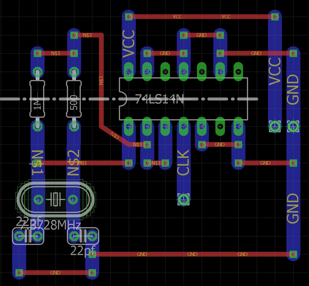
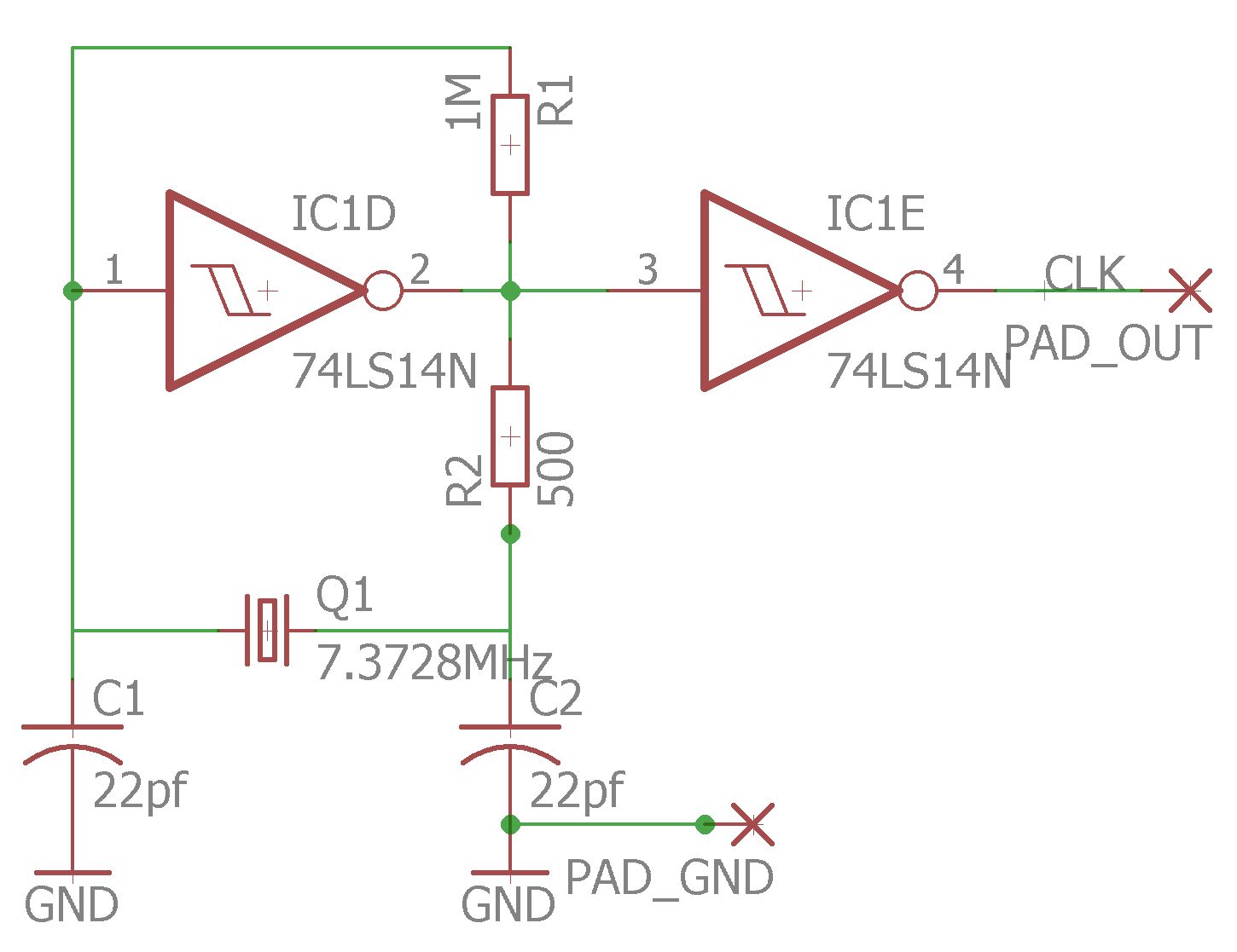
- You aren't powering the inverters!!
- Oh, wait, that's a error in the schematic. Still bad though. This error leads directly to:
- Because you aren't showing how the inverters are powered in the schematic, it makes it less obvious that you forgot the bypass cap.
Do it right. Show everything in the schematic, including how ALL the chips are powered. Digital chips like this need a bypass cap between their power and ground pins as close to the chip as possible. A 1 µF ceramic would do nicely.
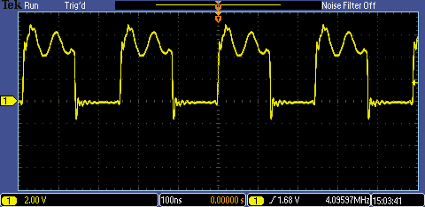
The fact that the tops of the waveforms are messy, but the bottoms clean, is a immediate clue that the mess is actually coming from the power.
Think about it. When the digital output is high, it's basically connected to Vdd via a FET of maybe a few 100 Ω at most. If there is crap on the output with nothing loading it, then that crap is coming from Vdd. Hmm. How did that get past bypassing at that frequency? Oh, look, there's no bypass cap! This really should have been a fairly obvious thought process.
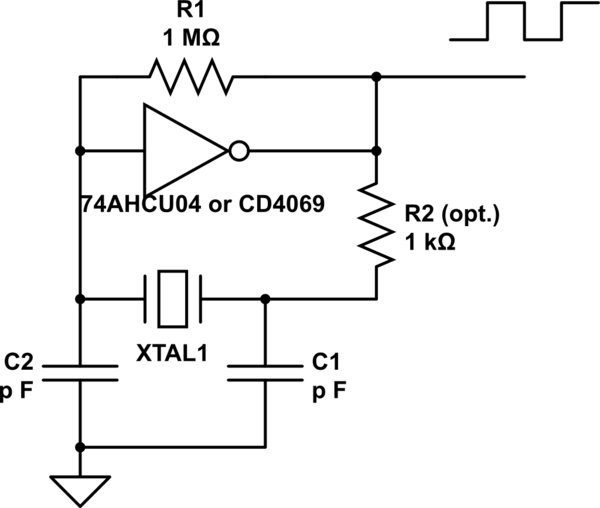
A additional problem is that you are using 74LS parts to drive the crystal. A 1 MΩ feedback resistor isn't going to do much across a 74LS inverter. The resulting hard edges are causing significant harmonic content out of the crystal, which is ringing so hard that it's polluting the power supply, which is helped along by deciding to leave off the bypass cap. It looks like your noise is the 4th harmonic, almost certainly caused by the crystal.
Use a CMOS inverter with balanced input levels (not TTL), add the bypass cap, and everything should be significantly cleaner.


