1
\$\begingroup\$

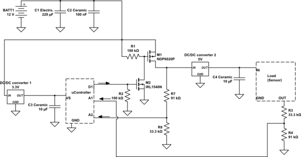
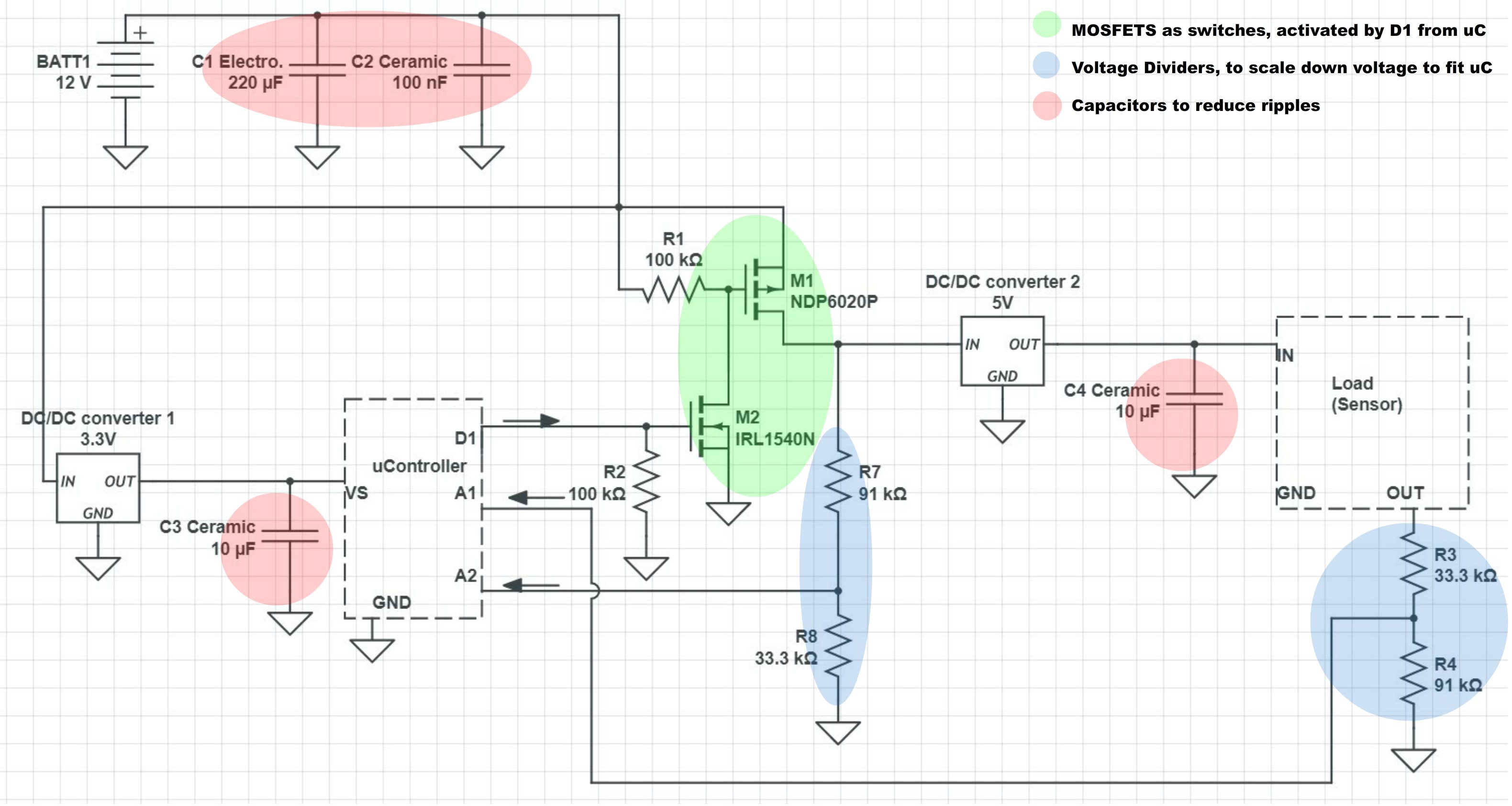
Could you please give me your feedback on following circuit?

.
schematic

simulate this circuit – Schematic created using CircuitLab
img Bigger image is available here

Explanation in brief:

Intention is to read a sensor value by a uC every 15 minutes and save as much energy as possible since it is going to be portable and battery powered. So I put uC in sleep mode when it's not reading. I also cut sensor power when uC is in sleep mode.

Procedure:

  1. uController is sending a signal through D1 to N-ch MOSFET (IRL1540G) >> P-ch MOSFET (NDP6020P) to turn on Load.
  2. Voltage is applied on Load (sensor) through buck converter
  3. Load (sensor) output, which is in range of 0.5V-4.5V and scaled down to maximum 3.3V, is going to A1.

.

Notes:

  • uC current consumption is 0.24 mA (sleep mode) to ~12 mA (up). Operating voltage is 3.3V.
  • Load current consumption is ~7mA. Operating voltage is 5V.
  • Buck converters quiescent current is 1.5mA , datasheet. But measuring by MM showed even lower at around 0.9mA.
  • Batteries are 3x26650 6A in series.  

  • uC is waking up every 15 minutes, for 5 seconds, to turn on sensor and read its value, and goes to sleep mode.

  • On A2 I'm reading battery pack voltage.

  • Based on my calculations it can run for around 13 months. Though I'm planning to use solar panels to prolong lifetime. That's why I'm feeding uC from 12V battery pack, and not AA batteries.

.

I would like to have your feedback and suggestions on followings:

  1. Are C3 and C4 values appropriate? Is it OK to use Ceramic capacitors, and not tantalum or other types?
  2. Do you have any suggestion on more-efficient buck converters with less quiescent current? or do you have any suggestion on reducing current consumption? Does it limit current consumption if I put a resistor after D1? or any suggestions in general?

.

Answering any of the questions is appreciated.

Thanks in advance

\$\endgroup\$
8
  • 7
    \$\begingroup\$ First and foremost read this: electronics.stackexchange.com/a/28255/41856 Fix it and then we'll talk. \$\endgroup\$
    – DerStrom8
    Commented Feb 1, 2018 at 19:11
  • 1
    \$\begingroup\$ r7 & r8 divider draws I=V/R = 12/(33.3k + 91k) ~= 96 uA. In one year this uses 96 uA x 8765 hours = 0.84 Ah. If battery is 6Ah this is .84/6 = 14% of battery energy in a year. Turning this divider off when not used increases battery life usefully. You can turn on a separate FET with 1 or just use M2 output which is close enough to Vbattery and read when sensor is enabled for a zero component count solution. \$\endgroup\$
    – Russell McMahon
    Commented Feb 2, 2018 at 6:13
  • 1
    \$\begingroup\$ 1.15 mA in sleep is much higher than many uCs achieve - what is the uC? \$\endgroup\$
    – Russell McMahon
    Commented Feb 2, 2018 at 6:14
  • 1
    \$\begingroup\$ You are missing the all-important description of what is this circuit supposed to do? You jump right into how you think it accomplishes whatever it's supposed to accomplish, but without a spec, that's context-free and therefore can only be skipped. The schematic layout is also rather confusing. Try to have logical flow left to right. Yours goes every which way for no reason at all. It took a little decoding to realize the two transistors at bottom left are apparently intended to switch the power to stuff at bottom right. Fix the mess. \$\endgroup\$ Commented Feb 2, 2018 at 12:09
  • 1
    \$\begingroup\$ @NimaSajedi - Yes M1 drain as you have now done. Diagram is MUCH better overall. || C3 is not TOO critical as long as converter noise is acceptable to uC. C4 value depends on need of sensor wrt noise and noise output of dcdc converter. It MAY be more critical to have good filtering on INPUTS of DCDC converters. Caps on inputs allow converter to respond to sudden load steps (if they exist). Caps on outputs also provide load step change current. You MAY benefit from a say 10 uF and a 0.1 uF in parallel - but modern ceramics may have low enough impedance at higher frequencies to serve ... \$\endgroup\$
    – Russell McMahon
    Commented Feb 3, 2018 at 11:17

1 Answer 1

2
\$\begingroup\$

Yes, what you show looks like it would do what you want. I didn't look at particulars since the text is too small to read after your latest edit. However, the basic topology looks sound.

Some things to consider:

  1. Make sure that the first FET is adequately turned on by the digital logic high voltage.

  2. Make sure the two voltage dividers properly attenuate the worst case input to the valid input range of the A/D.

  3. By "Vin" you apparently mean the supply voltage input?

  4. Check the quiescent current of the first DC/DC converter at left. A linear might yield lower long term average current if the micro spends most of its time sleeping.

\$\endgroup\$
1
  • \$\begingroup\$ 2. Do you mean that current that is going after voltage dividers is high enough to be detected by ADC pins? If so, it's done. 4. I found this one which has lower IQ. Could you please suggest me on C3 and C4 types and values as well? \$\endgroup\$ Commented Feb 2, 2018 at 20:11

Your Answer

By clicking “Post Your Answer”, you agree to our terms of service and acknowledge you have read our privacy policy.

Not the answer you're looking for? Browse other questions tagged or ask your own question.