15
\$\begingroup\$

I have somehow managed to make a little gizmo that primarily consists of an MCU, some sensors, and wireless connectivity. I have gone through the process of making the initial prototype, then designed a board and made an SMD version. It's small and it works nicely. It also has a nice case that I managed to 3d print then cover in a little homemade silicon sleeve. I made it for myself for fun but it works really well and everyone seems to want one. I could make maybe a few dozen of them by hand and sell them off to the people I run into that want one, but what if I run out quickly? It seems possible enough that I feel a little panicked at the thought, simply because I don't know where to start.

Where do I even begin to figure out how to take something to market? Is there a standard resource library for this sort of thing? I see no other question on the EE SE that asks quite what I'm asking (most people are looking looking for design or product advice, sigh, but I've already got that done), so maybe this is completely the wrong forum (another hint: I have no idea what to tag this), in which case I'd be happy to move it somewhere more appropriate.

Other pertinent info: I'm in the USA (NYC area) and possibly could be interested in shipping to other markets (Europe, possibly Asian markets) down the line.

Types of questions I am hoping to find advice for:

How do I find manufacturers for the different components (PCB, getting it soldered together, case, etc.)? Or maybe it's better put to say that I'm trying to find out how to shop manufacturers.

Should I split manufacturing to try to prevent IP theft?

Does the shop that assembles the boards also program them?

Certifications???

Marketing and distribution... ??? (I have a decent idea of how to get started here, but resources are always welcome)

Things I'm missing completely?

I feel like I know how to find what I need to engineer something and where to find general business advice, but the chasm between the two seems swampy and mysterious to me.

\$\endgroup\$
14
  • 2
    \$\begingroup\$ I'm voting to close this question as off-topic because this site is specifically intended for questions about electrical engineering theory and design. \$\endgroup\$
    – user80875
    Commented Jul 13, 2018 at 13:56
  • 6
    \$\begingroup\$ @CharlesCowie For EEs at small companies, dealing with production issues is not that unusual. Is there another forum that would be more appropriate? \$\endgroup\$
    – crj11
    Commented Jul 13, 2018 at 14:03
  • 7
    \$\begingroup\$ I concur with @crj11 on this. The answers to this question are all things that designers need to know as part of the product lifecycle. \$\endgroup\$ Commented Jul 13, 2018 at 14:07
  • 2
    \$\begingroup\$ I'm fine with the manufacturing question, but this particular question seems way broad. Frankly, with the 3D printed case and the homemade silicon envelope, this particular project would benefit from a thorough design-for-manufacturing pass before being ready for this type of discussion. \$\endgroup\$ Commented Jul 13, 2018 at 14:52
  • 2
    \$\begingroup\$ Also, a regulatory pass -- FCC, EU, ... \$\endgroup\$ Commented Jul 13, 2018 at 14:54

2 Answers 2

12
\$\begingroup\$

The topic police might close this, but this is actually a very reasonable question.

How do I find manufacturers for the different components (PCB, getting it soldered together, case, etc.)? Or maybe it's better put to say that I'm trying to find out how to shop manufacturers.

These are Contract Electronics Manufacturers (CEMs)

Without knowing where you are, I cannot help with specific companies, but I would expect there are some reasonably close. These companies usually have their own fabrication (PCB) vendors and supply chain kitting agents that they use and that will normally get you the best price.

Should I split manufacturing to try to prevent IP theft?

It will cost you more (typically) if you do. It is not uncommon for an NDA to be put in place. It is in the CEMs best interest to keep your design confidential (word gets around if they do not and that means they lose business).

Does the shop that assembles the boards also program them?

If you tell them how to and provide the programming files. You will be charged for the service as part of a larger quote.

Certifications???

Depends on where you intend to ship the units to. Europe has CE, USA has the equivalent (different versions of the same tests), as does Japan, Australia and New Zealand. You should look up the required certifications for your region.

The rest is determined by what you have and where you are.

Good luck.

[Edit]

Based on the discussion in meta, here are the various steps that have to be taken to get a product actually to market, each a valid question in its own right.

PCB manufacture. Most CEMs use their own sources as I noted, but you should ask for Design for Manufacturability comments. The PCB fabricators know what they can reasonably produce and can give helpful feedback to make the design better for them (and usually less expensive for you). This alone is a huge subject.

PCB Assembly: This is where the assembler can give likewise helpful comments (device spacing and host of other things). Once more a large question.

Design for test. This is also a question for the assembler; you would usually want them to test the device and the assembler knows what testing methods they prefer (there are many).

Programming; It may be that you have a suitable programming solution, or perhaps you can get the devices pre-programmed by the IC distributor (they will for a price provided the volumes are high enough) or you can ask the CEM to do the test. This is usually a quite long discussion.

Housing manufacture and product assembly. Sometimes the CEM will offer this service, and they can again answer questions about the most efficient method to achieve this.

Harnesses; there will be connectors and often cable harnesses which will need to be made; you could investigate your own sources or ask the CEM for suggestions.

Regulatory issues; I have mentioned some standards, but the entire area of compliance is complex and has many gotchas where experts really need to be asked their opinion. What are the regulations in my area and what does it take to pass them might be a good starting question here.

For the USA, you need to be wary of the fact that all 50 states (and many localities within them) have their own rules that may or may not impact your product. Once more, a discussion in its own right.

Obsolescence: A nasty word but one that is all too real in electronics - how would that be managed? (there are numerous methods including the CEMs who have subscriptions to parts intelligence databases).

Design for Bill of Materials. You may be buying a few bits from Digikey and co, but the CEM will want to buy from primary distribution and they will want to use reels, not a cut tape (for small devices) and tubes or trays for larger devices as their lines are designed for those things. You do not want the shock of finding that a diode you would like to use (or works in your prototype) has a minimum order quantity (MOQ) in distribution of 3000 parts on a reel. Another discussion in its own right.

There could be more but hopefully you can ask all the necessary questions; if nothing else it would be educational for both yourself and others.

Last but not least: the documentation pack. When I send a design out, the pack contains literally everything necessary to produce the design. This includes a master assembly drawing, a master PCB fabrication drawing (which contains information not in the gerber / ODB++ electronic data), drill drawings, test requirements, test methods with pass fail criteria, schematics (if you want the CEM to troubleshoot failed items), full production BoM (with all non populated parts removed).

Clearly, gerber / ODB++ data is sent as well (all the stuff necessary for the fabrication to be done). ODB++ is the preferred method for the better assemblers as of 2018.

My master assembly print also lists the identifiers of not fitted parts as they are usually still in the pick and place file (there are ways of ensuring they are not depending on the CAD tool used); if they are still in there, it is difficult for the CEM, so you need to help them out.

The documentation I provide meets IPC-D-325 incidentally.

I am not going to even get into export regulations.

Here is a (slightly redacted) fabrication master front page (page 1 of 3):
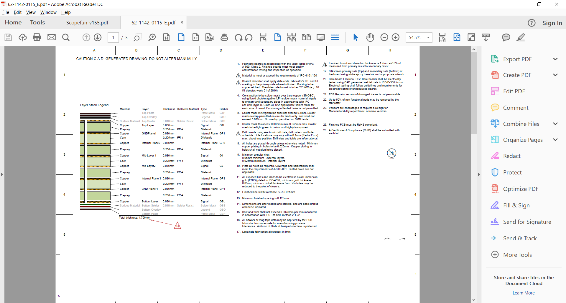
Fabrication Master drawing

\$\endgroup\$
5
  • \$\begingroup\$ Much appreciated and the answers are helpful, especially the linked resources. I'm in the USA (close enough to NYC), possibly could be interested in shipping to other markets down the line. I'll also add this to the question. If there are any other resources that you know of (links are extremely helpful) that help with this sort of stuff, it would be much appreciated. At this point I'm not 100% sure even what questions to ask. \$\endgroup\$ Commented Jul 13, 2018 at 14:46
  • \$\begingroup\$ Wow-- nice first pass!!! Sans wiki, Can we beef up your answer with some of the terms that might pop up in the contracting process? I know one issue that is useful to know about (there are hundreds!!) is turnkey vs fully or partially kitted assembly. The risk/ramifications re domestic vs offshoring would be another. Issues like who owns the tooling (if you need to make a mold) can also be quite surprising. \$\endgroup\$ Commented Jul 13, 2018 at 16:36
  • \$\begingroup\$ @ScottSeidman - go ahead an add as you desire; I know I have not covered everything and that there are lots of subtleties not yet addressed that are all very important. \$\endgroup\$ Commented Jul 13, 2018 at 16:38
  • \$\begingroup\$ This is so extraordinarily helpful, thank you so much. I was hoping to get a few starting sources to get a foothold, but this goes well beyond that. \$\endgroup\$ Commented Jul 13, 2018 at 16:57
  • \$\begingroup\$ @TrivialCase - we are happy to help (otherwise we would not be here) \$\endgroup\$ Commented Jul 13, 2018 at 17:09
2
\$\begingroup\$

You can find contract assembly houses, they don't have to be near to you, and if you contact various houses in India and China they are very eager to give a quote. many will offer small "jelly-bean" components for free as an incentive.

Splitting manufacturing is hard work for a small product, but it does make sense not to give away all the keys of the castle. Is there firmware? If so consider keeping that and the functional test stuff to yourself - at least at the start.

Your biggest headache by far will be certification (*). Anything that has signals over (from memory, but you need to look this up yourself and research it) 1MHz requires some form of conformance testing in both EU and US, and it isn't cheap. (You can risk going to market without it but you also then risk steep fines.) There are basically (at least) two forms of testing:

  1. Electrical safety testing. This applies to (again double check me) anything that has voltages over 30V DC or so. It immediately becomes a big deal the moment mains voltages enter the box. This is why so many products now run off "wall warts".

  2. EMI and RFI testing. This is actually two things. One is testing that the unit continues to work when subjected to various specified levels of interference. This can be either airborn (i.e. radiated signals from other equipment) or in the form of static charges delivered by the human hand. The other is testing that your unit does not emit interference above some specified level. This is immediately more of a deal the moment you have any form of transmitter.

All of this requires some fairly sophisticated equipment and expertise, and you do well to make friends with a reputable local test lab early in the design cycle. Some will let you do "pre-testing" to get a feel for what is required, at a reduced price. There are also numerous online resources. The actual certification testing is fairly expensive, typically several thousand dollars/day, so the trick is to do all you can to make sure you only have to do it once.

So you have some work to do to create a "product". More or less, and in no real order (in fact these tasks all overlap):

  1. do the actual design work, including board layouts, firmware, BOM's etc
  2. research what testing is required to enter the markets of your choice.
  3. perform and pass cerification testing to the standards you established above
  4. actually do a production run and do whatever QC you decided was necessary (above).

Naturally all this requires some investment in time and actual money. So you might be wanting to research something called "marketing" to ensure you get at least most of your money back. that is really beyond the scope of this post, but suffice it to say, it can involve as much work and investment as the design cycle itself.

Good luck!

(*) There is one workaround to the certification headache and that is marketing your product as part of a "kit". This is used by many small-medium businesses now. However, you still need to think about the potential effects of your device on others if something goes wrong. If, even accidentally or through misuse, your gadget causes bad things to happen, you might end up with major legal hassles (especially in the USA). So be sensible and ethical.

\$\endgroup\$

Not the answer you're looking for? Browse other questions tagged or ask your own question.