5
\$\begingroup\$

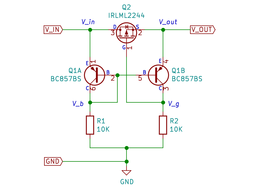
Below is an example circuit of an ideal diode (source):

ideal diode circuit

This circuit is easily found online, with various examples using resistor values ranging from ~1k to ~1M. I assume the reason for choosing higher value resistors is simply to reduce passive current drain, but going too high makes the circuit more susceptible to noise, or someone touching the circuit, etc. So my question is not about why bigger/smaller values are chosen.

My question is about the ratio between the resistor values. In some circuits I've seen, R1 = R2. In other cases, R1 < R2. However I've never seen an example circuit where R1 > R2; I don't understand why, and none of the example circuits I've found explain why they chose their particular resistor values.

My own intuition says it shouldn't matter if R1 > R2. As I understand it, V_b will simply be the higher of V_in and V_out, minus the V_be drop. If V_in > V_out (forward bias), then current flows from V_in to V_b, meaning Q1A is ON and Q1B is OFF, so R2 pulls V_g to GND, turning Q2 ON. If V_in < V_out (reverse bias), then current flows from V_out to V_b, meaning Q1A is OFF and Q1B is ON, so V_g = V_out (approximately), turning Q2 OFF. Conceptually, the function of R1 is to provide a current path for Q1A or Q1B to turn ON, and R2 is a pull down resistor for the gate of Q2; so I would think it doesn't really matter what the resistor values are, and R1 > R2 would be fine.

However I tested this circuit, and if R1 is sufficiently greater than R2 (see next paragraph), I found that the circuit does not work when a reverse bias is applied; current flows from V_out to V_in instead of being blocked like it should. Based on my explanation above, I don't understand why. I'm guessing my explanation is either wrong or incomplete, but I'm not sure what's wrong with my thinking.

In my test, my power supplies were set to 4.5V for V_in and 5.1V for V_out to create a reverse bias, and my circuit used the BCM857BS-7-F for Q1, the DMG2305UX for Q2, and 100k for R1. I used various values of R2, including 1M, 90k, 83.3k, 44.5k, and 9k (each achieved with various combinations of 10k, 100k, and 1M resistors that I had on hand). When using 83.3k or greater, the circuit worked as expected, and V_g was typically 5.0V, keeping Q2 OFF when applying reverse bias. With 44.5k for R2, V_g was about 2.2V, enough to keep Q2 always ON and make the circuit not work correctly with reverse bias. With 9k for R2, V_g was about 0.4V, again making Q2 always ON. This indicates that Q1B is partially ON instead of fully ON like it should be. I could understand that happening if h_fe had a value of like 10, but it's actually a minimum of 220 for this particular BJT, so I don't understand why there's a significant voltage drop from V_out to V_g.

Question 1 - Why does the circuit not work correctly in reverse bias when R1 > R2? (Or at least, when R1 is sufficiently bigger than R2.) Why is Q1B not fully turning ON?

Question 2 - Is there some ratio of R1 to R2 at which point Q2 is always ON, or does it depend on the exact components selected?

Question 3 - Is it safe to make R1 = R2, or is it better to make R1 < R2? My testing showed R1 can be at least slightly bigger than R2, but if the answer to Question 2 is "it depends", then I'm guessing that affects how safe it is to make R1 = R2.

New contributor
Fromen is a new contributor to this site. Take care in asking for clarification, commenting, and answering. Check out our Code of Conduct.
\$\endgroup\$
1
  • \$\begingroup\$ How will the MOSFET open if current direction is reversed? \$\endgroup\$
    – winny
    Commented 2 hours ago

3 Answers 3

3
\$\begingroup\$

The 2 transistors and resistors form a comparator. When VOUT is < VIN, Q1B turns off, and the FET turns on -- as desired.

If R2 < R1, then the comparator effectively has a positive offset -- so when VOUT is slightly > VIN, Q1B is still off, so the pass FET is on and the rectifier doesn't work as desired.

If the transistors are matched, the offset is approximately 26 mV*log10(R2/R1). So for a 2x ratio, you get 18 mV.

If R2 > R1, then the offset is negative -- you need VOUT slightly less than VIN to get the FET to turn on. Now, when it does turn on, the FET shorts VOUT to VIN, so the difference becomes zero, the FET turns off,...

==> The feedback loop needs some compensation -- usually the FET gate capacitance can supply that, but in some cases you may need a R in series with its gate.

\$\endgroup\$
1
\$\begingroup\$

[I]f R1 is sufficiently greater than R2..., I found that the circuit does not work when a reverse bias is applied; current flows from V_out to V_in instead of being blocked like it should.

Why does the circuit not work correctly in reverse bias when R1 > R2? (Or at least, when R1 is sufficiently bigger than R2

Q2 will be on / conducting as long as V_g is low enough. V_g depends on the current through R2 times the resistance of R2. For a given current, the smaller the resistance, the lower the voltage of V_g. The smaller the current, the lower the voltage of V_g.

When the drain and source of Q2 are at nearly equal potentials, Q1A and Q1B work as a current mirror. So, R1 and R2 will have similar currents. But the voltage drop across R2, being smaller, will be much smaller than the voltage drop across R1, so V_g will be low, and Q2 will be on.

Why is Q1B not fully turning ON?

I'm not sure "fully turning ON" is the right concept here. The voltage across Q1B depends on the current through R2. The question is not one of Q1B being "fully on", "partially on" or "fully off", but of how much current is flowing through it, and whether that amount of current is sufficient to cause a sufficient voltage drop across R2 to bring V_g high enough to turn Q2 off.

Is there some ratio of R1 to R2 at which point Q2 is always ON, or does it depend on the exact components selected?

Again, I'm not sure whether "ON" (or "OFF") is the right concept here.

Is it safe to make R1 = R2, or is it better to make R1 < R2?

Because component parameters can vary quite a bit, I would err on the side of making R1 < R2. Typically I see a ratio of R2 \$\approx\$ 1.5 x R1.

\$\endgroup\$
1
\$\begingroup\$

This arrangement, without the MOSFET, and with \$V_{OUT}=V_{IN}\$, is just a current mirror, where collector currents are approximately equal:

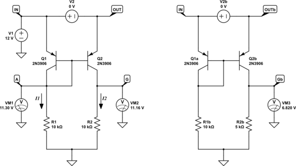
schematic

simulate this circuit – Schematic created using CircuitLab

Node G will eventually be used to control the MOSFET, which is absent for the time being. Sources V2 introduce a potential difference between IN and OUT, which I'll use later. Right now they are set to zero to obtain:

$$ V_{OUT} = V_{IN} $$ $$ I_2 \approx I_1 $$

Node A is held at \$V_{IN} - V_{BE} = +11.3V\$, so current \$I_1\$ is:

$$ I_1 = \frac{V_{IN}-V_{BE}}{R_1} = \frac{+11.3V}{10k\Omega} = 1.1mA $$ $$ I_2 \approx I_1 \approx 1.1mA $$

Being a current mirror, this equality between \$I_1\$ and \$I_2\$ is largely independent of R2, meaning that the voltage across R2 (potential \$V_G\$) will always be proportional to R2, according to Ohm's law:

$$ V_G = I_2 R_2 $$

In the case where \$R_2=R_1\$, both collectors will therefore have roughly the same potential, \$V_G \approx V_A\$, as shown above left on voltmeter VM2. The effect of altering R2 is to change this "quiescent" \$V_G\$. Assuming \$I_2\$ remains constant, reducing R2 will reduce \$V_G\$ in the same proportion. Halving R2 should halve \$V_G\$, as shown above right.

It's not an exact proportionality, because the equality \$I_2=I_1\$ is not entirely true; \$V_{CE}\$ for Q2 changes its current gain \$\beta\$, and transconductance \$g_m\$, but over a range of 10V or so, the change is only a few percent, and the approximation \$I_2 \approx I_1\$ is close.

In other words, R2 is chosen to set an appropriate gate potential \$V_G\$ when \$V_{OUT}=V_{IN}\$.

Symmetry is upset when \$V_{OUT} \ne V_{IN}\$. If \$V_{OUT}\$ changes even slightly (while \$V_{IN}\$ remains fixed), Q2's \$V_{BE}\$ also changes, which will destroy the mirror's balance, having a huge effect on \$I_2\$. It will no longer "mirror" current. If Q2 has transconductance \$g_m\$, you would expect a change \$\Delta V_{BE}\$ to cause a change in \$I_2\$:

$$ \Delta I_2 = -g_m \cdot \Delta V_{BE} $$

The corresponding change in \$V_G\$ would be:

$$ \Delta V_G = \Delta I_2 \cdot R_2 = -R_2 \cdot g_m \cdot \Delta V_{BE} $$

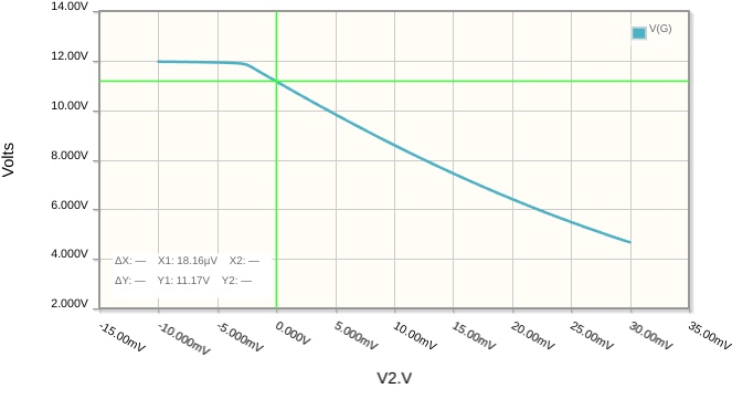
The purpose of voltage sources V2 and V2b in my schematics above, is to introduce that small change \$\Delta V_{BE}\$. They are set to zero above, so that \$V_{OUT}=V_{IN}\$, but I'll sweep that potential difference from -10mV to +30mV to observe the corresponding (much larger) change in \$V_G\$:

enter image description here

As you can see, when the two potentials \$V_{OUT}\$ and \$V_{IN}\$ are equal (vertical green marker), \$V_G=+11.2V\$. \$V_G\$ is the potential applied to the MOSFET gate, and this may or may not be an appropriate value. With the MOSFET in place, it would be controlled by \$V_{GS}\$, where:

$$ V_{GS} = V_G - V_S $$

In this application, source potential is \$V_S=V_{OUT}\$:

$$ V_{GS} = V_G - V_{OUT} $$

To switch the MOSFET on, you require \$V_{GS} < V_{GS(TH)}\$, so our "on" requirement is:

$$ V_G < V_{OUT} - V_{GS(TH)} $$

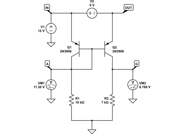
Let's say that the particular MOSFET in question has \$V_{GS(TH)} = -4V\$. In that case you might want to have the condition \$V_G \approx +8V\$ when \$V_{OUT}=V_{IN}=12V\$, so that it's just on the cusp of being switched on. Since current is \$I_2 = 1.1mA\$, you can calculate very roughly the necessary R2 to achieve that:

$$ \begin{aligned} I_2 &= 1.1mA \\ \\ R_2 &= \frac{V_G}{I_2} \\ \\ &= \frac{+8V}{1.1mA} \\ \\ &\approx 7k\Omega \\ \\ \end{aligned} $$

This assumes that current remains 1.1mA, which won't be the case due to the dependence of \$I_2\$ on \$V_{CE}\$, but it will be close enough for illustration:

schematic

simulate this circuit

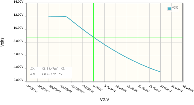
Sweep V2 again, and see how this affects \$V_G\$:

enter image description here

Now when the difference \$V_2 = V_{OUT}-V_{IN} = 0\$, gate potential \$V_G=+8.8V\$, much closer to the switching threshold of the MOSFET. Any change in this equilibrium, any difference between \$V_{IN}\$ and \$V_{OUT}\$, even only a few millivolts, will cause \$V_G\$ to swing fast to one side of that threshold or the other.

By changing R2 you can move \$V_G\$ to any potential you like (for \$0V < V_G < V_{OUT}\$), effectively allowing you to set the exact potential difference \$V_{OUT}-V_{IN}\$ at which the MOSFET is turned on. It's also possible to set \$R_2 > R_1\$, which will have the effect of saturating Q2 (when \$V_{OUT}=V_{IN}\$), and requiring \$V_{OUT}\$ to be significantly lower than \$V_{IN}\$ to switch on the MOSFET, but I don't see the utility of that in the context of this ideal diode implementation.

\$\endgroup\$

Your Answer

By clicking “Post Your Answer”, you agree to our terms of service and acknowledge you have read our privacy policy.

Not the answer you're looking for? Browse other questions tagged or ask your own question.