On semiconductor wafers there is a straight line, which is called Orientation Flat.

What exactly are these and how they are formed?
As stevenh says one of the purposes is to ensure correct orientation during handling. The other reason is to indicate the crystal orientation of the lattice and the wafer doping. From BYU's cleanroom website:
Wafer Flats
Purpose and Function
Orientation for automatic equipment
Indicate type and orientation of crystal.
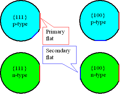
Primary flat – The flat of longest length located in the circumference of the wafer. The primary flat has a specific crystal orientation relative to the wafer surface; major flat.
Secondary flat – Indicates the crystal orientation and doping of the wafer. The location of this flat varies.
For large crystals no flats are ground. Instead a notch is machined for positioning and orientation purposes.
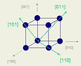
The crystal lattice is defined by how the wafer grew from the initial seeding.
It is important to cut the wafers along the crystal lattice if you want a clean break.

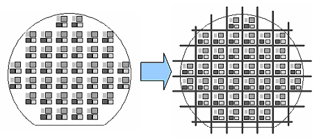
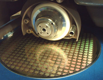
As their name suggests they're to ensure correct orientation during handling. If they were completely round there would be no way to know if the wafer wouldn't be slightly rotated, and then for instance in the process called dicing the saw would cut through all the dies. Which would be, er, pretty bad :-(.
The ingot the wafers are sliced from is cylindrical, and the wafers are originally round. The flats are created by cutting off a part of it.


Orientation Flat is usually formed by grinding one side at the boule level. XRD measurments are used to check crystal orientation.
Certain semiconductor devices (edge emitting lasers in particular, but also SOA, SLED, PICs) are formed by cleaving wafers to dies after processing = breaking them along crystal planes.
There are also substrates / wafers with Precision Flats = cleaved flats (not grinded), which are made to ensure precise alignment of devices along crystal planes, which then help to obtain clean cleave, which is later coated with reflective or antireflective dielectric layer stacks, to make mirrors for lasing = edge emitters (lasers, SOA, DFB, DBR).