4
\$\begingroup\$

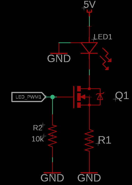
I am making a simple LED PWM brightness control circuit. I am using a relatively high power White CREE LED, N-channel Enhancement MOSFET BSS316N and Resistor R. The circuit is as shown below.

PWM Circuit

I am driving the Gate of the N-channel MOSFET with a 3.3V, 100KHz PWM from a microcontroller.

The CREE LED which I am using is rated for 1A and after testing it (With a 5V constant DC supply and resistor in series with the LED), I am happy with the brightness I got from the LED when the average current passing through it is around 350mA. So I want to drive this LED around this current rating(also because of thermal considerations for long life. 1/3rd max current rating). So for a current of 350mA, 5V supply and 3.05V forward voltage of the LED, the current limiting resistor comes to around 6Ω(1W resistor).

Now when I wire up the PWM circuit as shown in the image above, with R1=6Ω and a 3.3V, 100KHz, 90% duty cycle signal at the gate and 5V DC supply, the average current measured(directly from the DC supply or reverse calculation from voltage across the current limiting resistor, R1) comes to around 60mA and not the 350mA I designed for. So the LED is dimmer than when it is driven at an average current of 350mA. I presume this is due to the PWM drive.

Now question is how should I mathematically calculate R1 for a particular average current and a particular duty cycle so that I get my desired brightness(when average current is 350mA). I can practically keep changing R1 to lower values till I find the correct value, but shouldn't there be a better way?

So if I use a lower R1 value, Avg current will drop in case of PWM drive, but I am sure impulse current will be higher. Can this potentially damage the LED in the long run?(Switching Freq: 100KHz) or is it acceptable?

PS: I am not looking for a constant current driver circuit solution.

\$\endgroup\$
4
  • \$\begingroup\$ Fix +5V tied to GND err. \$\endgroup\$
    – D.A.S.
    Commented May 15, 2019 at 14:13
  • 2
    \$\begingroup\$ That's a thermal pad, if I understood your crib correctly. \$\endgroup\$
    – dev_000
    Commented May 15, 2019 at 15:03
  • \$\begingroup\$ i see ok then.. \$\endgroup\$
    – D.A.S.
    Commented May 15, 2019 at 16:05
  • \$\begingroup\$ Current limiting resistors or circuits like the one you provided tend to be important to keep an LED stable and consistent. To that end you want to pick a size that handles your voltage variation, component variation and operating temperature variation properly. You want enough resistance so that at the maximum operating temperature of the circuit at the maximum operating voltage, on the diode with the lowest threshold voltage the LED isn't damaged, while at the lowest voltage at the lowest operating temperature with the highest threshold voltage it's still sufficiently bright. \$\endgroup\$ Commented May 15, 2019 at 21:08

3 Answers 3

5
\$\begingroup\$

PS: I am not looking for a constant current driver circuit solution.
And yet as pointed out in other answers what you have unintentionally built is a crude current sink.

If you just want to use the mosfet as a switch then (as other answers have said) the source of the mosfet needs to be connected to ground and the resistor needs to go between the mosfet and the LED (or between the LED and the 5V supply).

Can you please elaborate as to why it behaves as such? (as a current sink)

The current through the mosfet depends on the voltage between the gate and the source, but your gate is no longer grounded.

This sets up negative feedback, as the current in the resistor increases the voltage across the resistor increases which means the voltage between the gate and the source decreases.

Unfortunately predicting what the current will be is non-trivial. There is a graph of typical forward characteristics in the datasheet but.

  • It shows huge temperature dependence.
  • It's only valid for VDS > 2V.
  • It's only typical.
  • Reading precise values off graphs is never easy.

Looking at the 25C graph it suggests that at the currents we are working at there will likely be about 2.5V across the gate.That would leave about 0.8V across the resistor and a current in the resistor of about 133ma.

Your measured value is about 50% of this, there may be several things contributing to this discrepancy.

  • You are PWMing, your multimeter is likely measuring the average voltage not the peak.
  • The drain-source voltage is probablly more like 1V than, 2V. This may require a higher gate-source voltage to acheive the current.
  • The "3.3V" output from your microcontroller may well not be a full 3.3V.
\$\endgroup\$
1
  • \$\begingroup\$ Thanks for the clarification. \$\endgroup\$
    – dev_000
    Commented May 15, 2019 at 15:58
6
\$\begingroup\$

The resistor in series with the source isn't allowing the MOSFET to turn on completely, you need to move the resistor in series with the source to the top, in series with the LED.

\$\endgroup\$
2
  • \$\begingroup\$ Thanks for letting me know the error. Can you please explain as to why it's not turning ON with resistance between source and ground so that it gets documented as a proper answer. \$\endgroup\$
    – dev_000
    Commented May 15, 2019 at 15:02
  • 1
    \$\begingroup\$ For an N-channel MOSFET, it is the voltage from gate to source that turns it on. So, anything in series with the source that can drop voltage will interfere. 300 mA * 6 ohms = 1.8V, so now your gate voltage relative to ground needs to be higher. As you can see, you don't get 300 mA, an equilibrium somewhere is found at a lower current (and lower source resistance voltage drop). \$\endgroup\$
    – Mattman944
    Commented May 15, 2019 at 15:08
3
\$\begingroup\$

Now question is how should I mathematically calculate R1

You did a fine job calculating the value but a crappy job in its placement. It needs to go directly in series with the LED and not in the source of the MOSFET.

Once you put it in the source, the MOSFET behaves like a constant current circuit and you force a much lower voltage across the source resistor. Your numbers imply to me a value of 0.36 volts and that tallies with the VGS(threshold) value for most common MOSFETs and the drive level of 3.3 volts on the gate.

\$\endgroup\$
1
  • \$\begingroup\$ Can you please elaborate as to why it behaves as such? \$\endgroup\$
    – dev_000
    Commented May 15, 2019 at 15:03

Your Answer

By clicking “Post Your Answer”, you agree to our terms of service and acknowledge you have read our privacy policy.

Not the answer you're looking for? Browse other questions tagged or ask your own question.