6
\$\begingroup\$

Basically what the title says. Cadmium is a toxic, environmentally harmful heavy metal that's banned under the RoHS directive, and even before RoHS its toxicity was well known. What makes cadmium selenide and cadmium sulfide such appealing semiconductors to make photocells out of?

Why not use silicon, which also drops in resistivity when exposed to light? Silicon does even respond to most visible light as far as I'm aware, though not as strongly as CdS/CdSe due to being an indirect bandgap semiconductor. But other direct bandgap semiconductors exist, too, including ones without any highly toxic elements, like gallium antimonide or tin sulfide, or any of the more complex compounds used for thin-film solar cells. What gives cadmium compounds such an advantage?

\$\endgroup\$
3
  • 1
    \$\begingroup\$ Dude. They used cadmium by the righteous boatload for rechargeable batteries. The sprinkle of cadmium needed for a photocell doesn't even count against that. \$\endgroup\$
    – JRE
    Commented May 28, 2019 at 15:35
  • \$\begingroup\$ @JRE Sure, but the moment there was a good alternative available they switched pretty much completely to NiMH. \$\endgroup\$
    – Hearth
    Commented May 28, 2019 at 15:37
  • 2
    \$\begingroup\$ Probably because their peak sensitivity wavelength is close to that of the human eye and they do, overall, do a reasonable job of approximating human sensations of brightness. (Silicon is too responsive to IR and deep red light for some uses.) Plus, they've been in use a very long time and many of the systems installed decades ago are still working and meet their original specs when installed. That long successful experience might trump something with less time in practice (in some cases, anyway.) It's cheap and easy to make with low-tech and I'd guess probably not going away any time soon. \$\endgroup\$
    – jonk
    Commented May 29, 2019 at 5:18

4 Answers 4

7
+150
\$\begingroup\$

What makes cadmium selenide and cadmium sulfide such appealing semiconductors to make photocells out of?

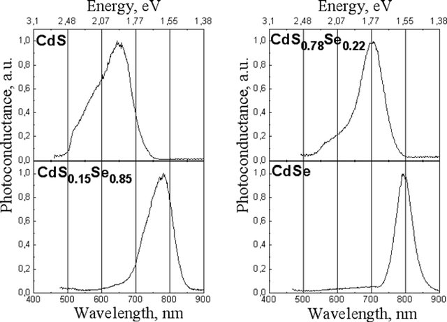
Cadmium sulfide and Cadmium selenide turn conductive in the visible wavelengths, they do this because they are semiconductors and the bandgap is responsive to visible wavelengths.

A photoresistor is made of a high resistance semiconductor. In the dark, a photoresistor can have a resistance as high as several megohms (MΩ), while in the light, a photoresistor can have a resistance as low as a few hundred ohms. If incident light on a photoresistor exceeds a certain frequency, photons absorbed by the semiconductor give bound electrons enough energy to jump into the conduction band. The resulting free electrons (and their hole partners) conduct electricity, thereby lowering resistance. The resistance range and sensitivity of a photoresistor can substantially differ among dissimilar devices. Moreover, unique photoresistors may react substantially differently to photons within certain wavelength bands. Source: Wikipedia Photoresistor

enter image description here Source: Optical and photoelectrical properties of CdSxSe1-x films produced by screen-printing technology

But other direct bandgap semiconductors exist, too, including ones without any highly toxic elements, like gallium antimonide or tin sulfide, or any of the more complex compounds used for thin-film solar cells. What gives cadmium compounds such an advantage?

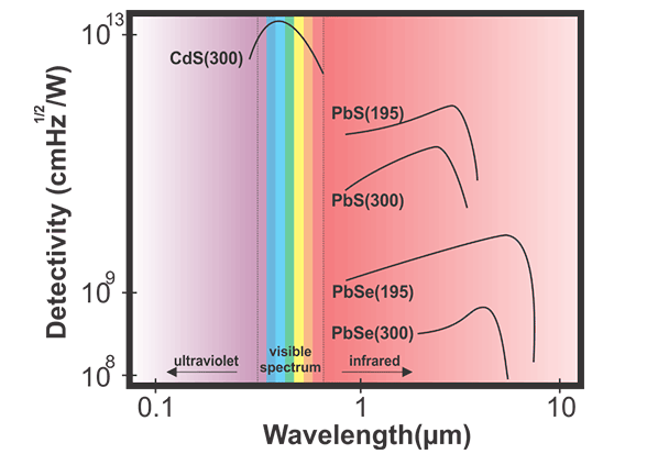
There are other materials that are responsive, but CdS or CdSe have responsivity in the visible wavelength range, this is useful if you want your device to respond in the same wavelength range that people see in. CdS is the best photosensitive material in the visible range and photodetectors made from CdS are cheap. The alternative would be a photo diode circuit, which is more complex and requires more components.

enter image description here
Source: http://www.resistorguide.com/photoresistor/

\$\endgroup\$
4
  • \$\begingroup\$ Are there any nontoxic alternatives? I would think you could use any of the same sorts of materials used for photodiodes for this, no? \$\endgroup\$
    – Hearth
    Commented May 30, 2019 at 21:07
  • \$\begingroup\$ I haven't seen any, I don't think there are any good material substitutes for CdS. I think modern integrated circuits make photocells irrelevant. Now you can build a diode based photodetector in the same device size, although the cost is more \$\endgroup\$
    – Voltage Spike
    Commented May 30, 2019 at 22:53
  • \$\begingroup\$ I have seen some Chinese devices that are photodetector replacements, as far as I can tell they are photodetector circuits \$\endgroup\$
    – Voltage Spike
    Commented May 30, 2019 at 22:57
  • \$\begingroup\$ As the most complete answer here, I'll give this one the bounty. I'm not really 100% satisfied (a bit of an explanation of that last graphic might be nice?) but I think this covers all the main points. Where do other materials not based on lead or cadmium fall on that graph? \$\endgroup\$
    – Hearth
    Commented Jun 3, 2019 at 16:34
2
\$\begingroup\$

First, they were first. As a useful photoresistive material, cadmium et. al. predates silicon devices by decades.

Second, they are not semiconductors. This is one of the main reasons why they are still in demand in areas such as professional audio.

Third, the property change (resistance in this case) from dark to light (dynamic range) is huge. This means that many applications do not need any amplification or other signal processing.

Fourth, they can be made to handle high (compared to silicon devices) voltages, such as offline TRIAC gating.

Fifth, reliability.

\$\endgroup\$
5
  • \$\begingroup\$ They're not semiconductors? That's news to me. And contradicts my understanding of how they even work. Can you provide citations for your claims here? What makes them more reliable? How can they handle higher voltages than silicon? How does the dynamic range compare to alternative devices? \$\endgroup\$
    – Hearth
    Commented May 28, 2019 at 14:55
  • \$\begingroup\$ CdSe is a class II-IV semiconductor en.wikipedia.org/wiki/Cadmium_selenide CdS also has a bandgap en.wikipedia.org/wiki/Cadmium_sulfide \$\endgroup\$
    – Voltage Spike
    Commented May 28, 2019 at 15:58
  • \$\begingroup\$ I took the term "photocell" to mean a photoresistor, not a solar cell or any other Cds use. In that context, CdS has no directionality or polarity. Whatever its underlying physics, it does not "behave" the same way a photodiode or phototransistor does. \$\endgroup\$
    – AnalogKid
    Commented May 28, 2019 at 16:43
  • \$\begingroup\$ @AnalogKid I am referring to a photoresistor. That doesn't make it not a semiconductor. The way it works is in fact completely predicated on carrier pair generation by photon absorption; an electron in the valence band absorbs a photon and becomes a free electron-hole pair, and since conductivity is proportional to the carrier concentration, conductivity increases as more carrier pairs are generated. Importantly, this is a defining characteristic of semiconductors; this type of carrier generation does not occur in metals or insulators. \$\endgroup\$
    – Hearth
    Commented May 28, 2019 at 20:48
  • \$\begingroup\$ @analogkid the bandgap changes the resistance in CdS the mechanism is not the same as transistors, it is still a semiconductor. When a photon hits CdS, it jumps the bandgap and current flows \$\endgroup\$
    – Voltage Spike
    Commented May 30, 2019 at 22:47
2
\$\begingroup\$

More a complement to other answers than a full standalone one. One of the aspects which I would like to stress about those devices, apart from their ruggedness and inexpensivess, is that they exhibit a more linear behavior respect to other semiconductor devices when operated as controlled resistors.
This characteristic is fully exploited for example by Jim Williams in his design of an ultra-low distortion audio frequency Wien bridge sine oscillator ([1], pp. 29-32). By using a VACTEC VTL5C10 or a CLAREX CLM410 LED/photoresistor coupler instead of a 2N4338 with local feedback, he succeeds in eliminating the resistivity voltage modulation in the amplitude control feedback loop of the circuits of figures 45 and 47, removing a significant amount of distortion (compared to the already low values he achieves) from the output waveform. This is due to the fact that in photoresistors the conduction is ohmic, without any diffusive components, which are instead of paramount importance for example in JFETs (in this respect, see my answer to the question "How current is steady after pinch off voltage?").

Final considerations on the inexpensiveness of CdS/CdSe photoresistors. The main characteristic of inexpensiveness of these devices is achieved because CdS and CdSe, despite being semiconductors exactly as GaAs and GaN, need not to be grown as a monocrystalline structure for those applications. Their high basic resistivity is not affected too much by the polycrystalline structure they assume when deposed on insulating or metal substrates by sputtering, vapor deposition or other similar techniques, in order to produce photoresistors. This is a far more economic production process respect the ones required by other semiconductor photodevices.

Reference

[1] Jim Williams (July 1990), "Bridge Circuits Marrying Gain and Balance", Linear Technology Application Note 43, pp. 48.

\$\endgroup\$
1
\$\begingroup\$

As long as EU maintains a Cadmium exception for PV modules and sensors, etc in RoHS, they are still available. These exemptions came with a promise to setup recycling routes.

What makes cadmium selenide and cadmium sulfide such appealing semiconductors to make photocells out of?

Inexpensive sensors with a very high sensitivity of 0.8-Ω/Lux spanning many decades, avoiding the need for amplifiers.

\$\endgroup\$

Your Answer

By clicking “Post Your Answer”, you agree to our terms of service and acknowledge you have read our privacy policy.

Not the answer you're looking for? Browse other questions tagged or ask your own question.