To answer this question, it is necessary first to recall the form of the current density in a semiconductor device according to the customary Drift-Diffusion model, then to see what's happen precisely in a JFET: I apologize for not being elementary, but the answer requires some concepts which, I hope, I'll made understandable.
The current density across the channel transversal section of a JFET. Since the JFET, as all Field Effect devices, is a majority carrier device, let's consider a \$n\$-channel JFET and see that the biggest contribution to the current density is due only to the motion of electrons (call it \$J_n\$), which has the following form
$$
J_n=\underbrace{q\mu_n nE}_\text{Drift}+ \underbrace{qD_n\nabla n}_\text{Diffusion}\label{1}\tag{1}
$$
where
- \$q \$ is the elementary electron charge,
- \$n\$ is the conduction electron density in the region considered,
- \$E\$ is the electric field applied to the device,
- \$\mu_n\$ and \$D_n\$ can be considered as proportionality constants and their meaning is not useful to this discussion, so we'll not describe it.
The current density consist of two contribution of very different nature. Without giving too many details, we can say that the drift term at the right side of equation \eqref{1} identifies a ohmic (i.e. resistive) contribution since is proportional to the electric field (and thus the the voltage applied to the device) and its magnitude depends on the availability of electrons and thus on the magnitude of \$n\$ in a given region. On the other hand, the diffusion term is proportional to the magnitude of variation of the charge density \$n\$ trough its gradient \$\nabla n\$, and not on the magnitude of \$n\$ itself.
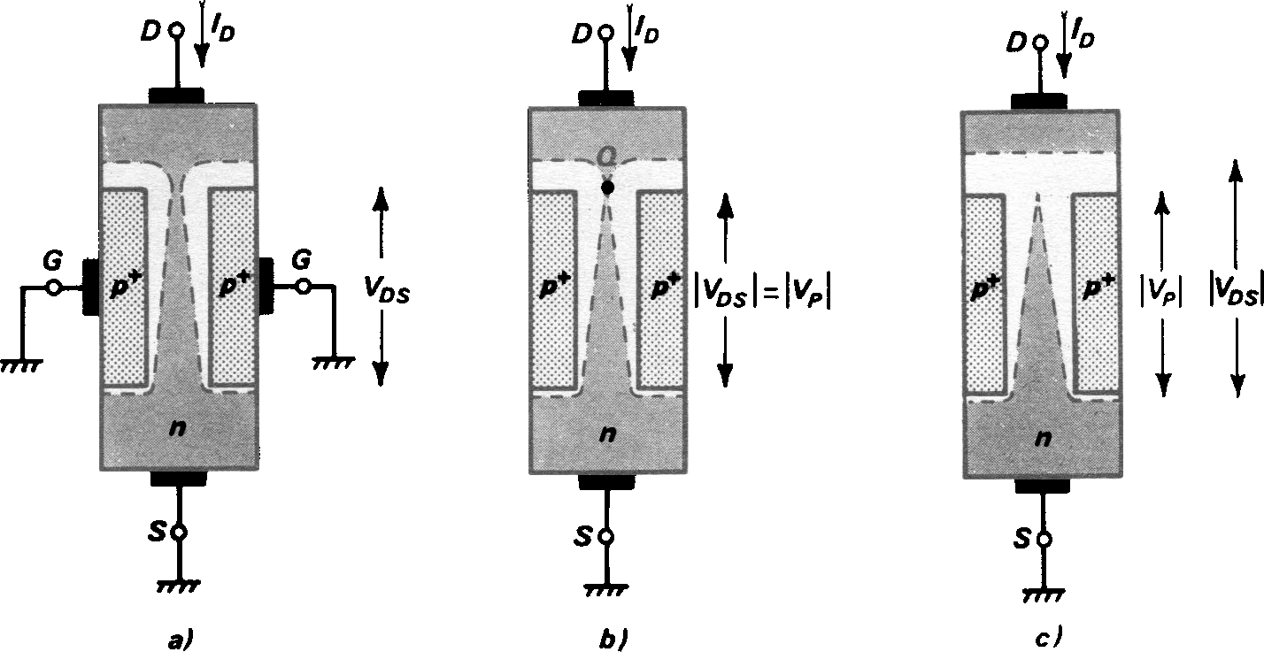
What happens in a JFET at Pinch OFF? Let's consider the qualitative behavior of the current conduction by using the following picture, where it is supposed \$V_{GS}=0\mathrm{V}\$ for simplicity and without restriction to generality.

Let's call \$V_P\equiv V_{GS_\mathrm{th}}\$ the thresold or pinch-off or ON gate voltage the voltage that should be applied to between the gate and the source of the JFET in order to bring to (almost) zero its drain current.
- In a) we have \$V_{DS}<V_P\$ and the depleted region near each gate-channel \$pn\$ junction increases its width when moving from the source to the drain terminals, where the conduction electron charge density \$n\$ is nearly \$0\$. However, this region does not yet extend in such a way to fill the whole channel section: there is still a conduction path between the source and the drain, thus the dominating contribution to the drain current is given by the drift term in \eqref{1} and \$I_D\$ rises almost proportionally to \$V_{DS}\$.
- In b) we have exactly \$V_{DS}=V_P\$, thus there exists a full channel section of the JFET where \$n\simeq 0\$: the drift contribution to the drain current ceases to be the main one, and is in fact reduced consistently. However \$I_D\$ does not ceases because the diffusion term in \eqref{1} becomes very high since, near the depleted section of the channel, there is a very strong variation of \$n\$ as it goes to its doping defined level to almost zero very quickly and this implies \$\nabla n\gg0\$.
Thus \$I_D\$, from now on, is almost independent on the rise of \$V_{DS}\$ since the main contribution to its magnitude is the diffusion term that does not depend on the applied drain voltage. This is depicted in part c) of the picture which shows that, during the rise of \$V_{DS}\$ above the \$V_P\$ value, a greater part of the channel region becomes depleted, however influencing little the value of \$I_D\$ due to the fact that \$\nabla n\simeq \text{const.}\$ and due to the relative magnitude of the two terms in \eqref{1}.

