0
\$\begingroup\$

There is a design of a circuit proposed in the following way:
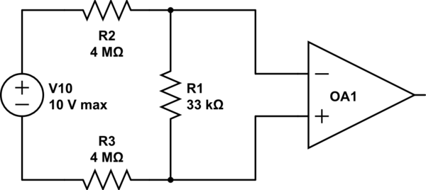
schematic

simulate this circuit – Schematic created using CircuitLab

The amplifier has a gain of 80, on R1 when the input voltage is equal to 10 V, it will be approximately 41 mV and when amplified by the OP would have 3.3V, which is the maximum volatje of the ADC of an MCU.

Could there be some kind of problem with this design?

The idea of using the voltage divider is to prevent the negative terminal of the voltage source (0 to 10V) from being connected to the ground of the main circuit, ie to isolate it in a certain way.

\$\endgroup\$
12
  • 1
    \$\begingroup\$ whether that will be sufficient depends on the rails that OA1 uses, what its input common mode voltage range is, what the potential between the grounds is, and whether it has a low enough common mode input impedance. Unless all those are valid together, you may well be outside its common mode input voltage range, which is not going to work. You either need to define the voltage difference between the two circuits by some suitable connection, or use a different topology for OA1. \$\endgroup\$
    – Neil_UK
    Commented Jun 14, 2019 at 16:22
  • \$\begingroup\$ can you elaborate on what is your voltage source? \$\endgroup\$
    – devnull
    Commented Jun 14, 2019 at 16:24
  • \$\begingroup\$ Thanks for writting. The input source is undefined, it can be a temperature or pressure sensor, anything that a user can connect and its voltage is variable between 0 to 10V. Is there a circuit or design that is better to measure this voltage? \$\endgroup\$ Commented Jun 14, 2019 at 16:28
  • 1
    \$\begingroup\$ What's the goal? Dividing by 250 and then mutiplying by 80 is going to introduce noise to the signal. What are you trying to get in return? \$\endgroup\$
    – The Photon
    Commented Jun 14, 2019 at 16:31
  • 1
    \$\begingroup\$ Please let us know if what Neil_UK commented is not clear for you. Common mode voltage is very important. "Undefined" voltage sources may (or may not) work on simulations with ideal components but real circuits have many important issues you should be concerned about. \$\endgroup\$
    – devnull
    Commented Jun 14, 2019 at 16:33

2 Answers 2

1
\$\begingroup\$

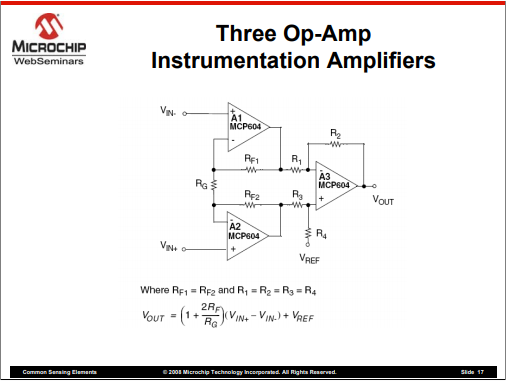
I think one solution is the following:

enter image description here

Obviously, it is necessary to calculate the values of the resistors for which, instead of amplifying the signal, it is attenuated for the correct values of the ADC of the MCU.

\$\endgroup\$
0
\$\begingroup\$

The question is lacking the common mode voltage rejection ratio limited now by the resistor tolerance errors from a perfect balanced differential source that may be imperfect due to cable unbalance to stray EM fields. It is also lacking the required BW and filtering to reject CM noise and the desired SNR of the reading captured by the ADC.

With more details on the electrical noise environment , layout of signals and noise with the above missing specs, a better review of your proposed solution is possible.

Thus using 1% resistors you have degraded the CMRR from >100 dB to <=34 dB worst case

\$\endgroup\$

Your Answer

By clicking “Post Your Answer”, you agree to our terms of service and acknowledge you have read our privacy policy.

Not the answer you're looking for? Browse other questions tagged or ask your own question.