This question would be much easier to answer if you had provided a link to the datasheet so we could read the specification for ourselves. However ...
The IC accepts a high impedance input ...
This is most likely incorrect interpretation. The usual configuration is that the IC presents a high impedance to the circuit that is driving it. That means that it will require very little current to control the enable input.
... (can't be pulled to any voltage) to enable operation, ...
This should possibly read "can be left floating to enable operation". This suggests that the enable input has an internal pull-up resistor to force a logic high if it is left unconnected.
... or it can be pulled down to disable operation.
This bit is correct. A simple connection to ground using a transistor, GPIO, etc., will do the trick.
However I want it to operate in an inverted way, where a 0V input will result in the output being pulled down and 3V3 input will give a high impedance output.
0 V pulling the input down is not inverted - it is direct connection. If the chip accepts 3V3 logic then you just directly connect your signal to the enable input. If not then you may need a logic level converter.
- 0 V in will disable the chip.
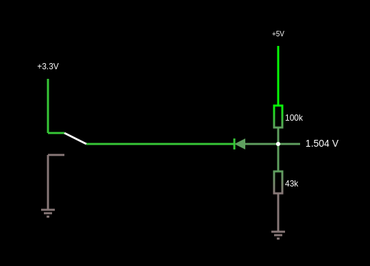
- 3V3 in will drive the high impedance input of the chip high using the low impedance of your source signal.
In general, we use low impedance sources to drive high impedance loads. This way one output can drive multiple inputs.
From comments:
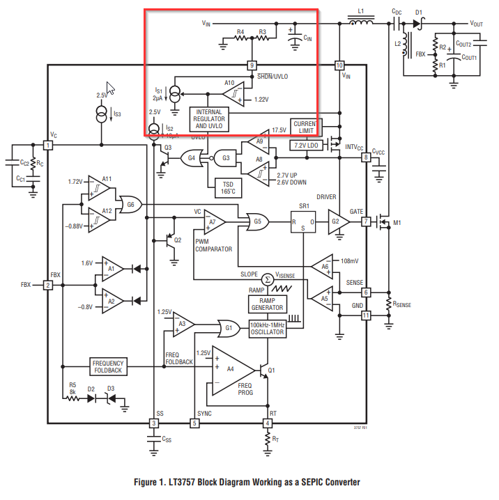
I'm talking about the 'SHDN/UVLO' pin. In normal operation, it's used for undervoltage detection and should not be influenced (hence I need to apply a high-impedance load). When shut down is desired, it should be pulled low.

It's clear from Figure 1 that SHDN/UVLO is an input so it is the load, not the voltage divider to the pin (which is the source). You just need to take into account that it is trying to take 2 μA from the divider.


