2
\$\begingroup\$

I am designing a solar charger with MPPT for a 1-cell lithium polymer battery of approximately 6000 mAh. The solar panel is 10W and 21 Voc.

I am trying to ensure that the charger has protection against reverse voltage for both the solar panel and the battery.

My questions are focused on the protection of the battery against reverse voltage, not on the design of the charger itself. The complete scheme can be seen below.

Complete schematic

The battery protection circuit is extracted from this Analog Devices document but with some modifications.

In summary, the operation is as follows:

Q2 and Q3 provide a reverse voltage detection circuit and Q4 is the one who disables the battery. If the battery polarity is correct, Q2 and Q3 are cut-off and therefore, Q4 connects the battery. In the event that the battery is connected in reverse, Q2 and Q3 are activated and then shunt the gate of Q4 to ground, causing Q4 to break and the battery is disabled. Do you see any fault or something that can be improved?

Datasheets:

Thanks and best regards.

\$\endgroup\$
1
  • 1
    \$\begingroup\$ Two notes: 1. I would suggest not using a ground symbol for VBatt-. Using the same symbol for different grounds implies they are the same reference. 2. If you know the solar panel can output 21v, then the electrolytic caps should be twice this and the next typical voltage, so 2*21v = 42v --> 50v caps. \$\endgroup\$
    – rdtsc
    Commented Sep 18, 2019 at 14:56

1 Answer 1

1
\$\begingroup\$

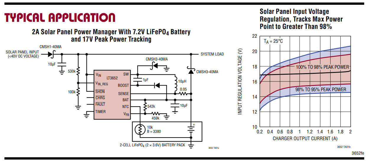
You've made a mess of the charger circuit: -

enter image description here

Your "switch" node doesn't have a schottky diode to ground and it appears that your boost capacitor is inappropriately connected.

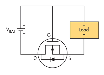
It looks like your reverse battery protection will work but why over-complicate a reliable standard circuit such as this one: -

enter image description here

Is it because of the charger circuit might keep the MOSFET activated and drain the battery?

\$\endgroup\$
2
  • \$\begingroup\$ Oops, you're right, I'll correct the design of the charger. Thank you. Complicating the design is because in the solution that you have proposed, if the input power connector is attached and the charger is on, then the charger produces a voltage from the gate to the source of the NMOS and it becomes active. It would be correct? \$\endgroup\$ Commented Sep 18, 2019 at 14:47
  • \$\begingroup\$ I thought that must be the reason. \$\endgroup\$
    – Andy aka
    Commented Sep 18, 2019 at 14:52

Your Answer

By clicking “Post Your Answer”, you agree to our terms of service and acknowledge you have read our privacy policy.

Not the answer you're looking for? Browse other questions tagged or ask your own question.