1
\$\begingroup\$

I would like to know how do we choose the nodes for a Thevenin Equivalent Circuit.

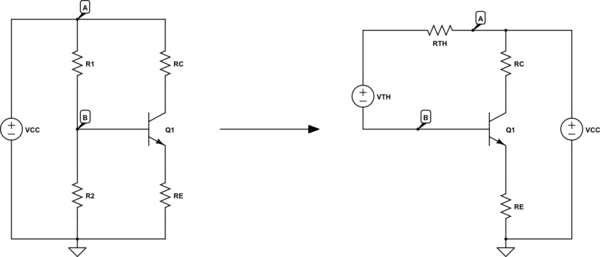
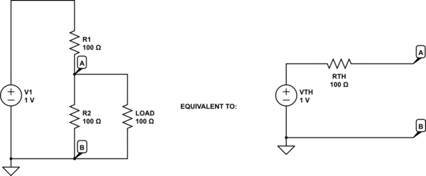
For example, in the voltage divider, we compute the Thevenin equivalent circuit between the nodes where we would connect our load:

schematic

simulate this circuit – Schematic created using CircuitLab

(do not mind the value of the voltages and components, they are irrelevant for my question in addition to be wrong because I haven't done the calculations).

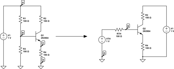
However, in an amplifier circuit (for example, a simple common-emitter), I do not understand how do we choose the nodes for the equivalent circuit:

schematic

simulate this circuit

We use for example a thevenin equivalent circuit to easily compute the biasing base current of the transistor. What nodes do we choose for that? As the resulting equivalent circuit is connected between the base and the ground, I assume it was computed between these nodes (nodes B and D), is it correct?

This case is similar to the voltage divider, however what do we consider being our load? As we computed the equivalent circuit between B and D, does it mean that our load is the base-emitter junction along with the emitter resistor?

Why have we not chosen to compute the equivalent circuit between nodes A and B for example? Would it be possible and would we get the same results?

Thank you.

EDIT: after having thought about this and redone the calculations, it seems that the two solutions are equivalent:

Taking the Thevenin equivalent between nodes A and B gives:

schematic

simulate this circuit

Here we have \$ V_{TH} = \frac{R1}{R1 + R2} V_{CC} \$ and \$ R_{TH} = R1 // R2 \$.

KVL gives us: \$ V_{CC} = R_{TH}.i_b + V_{TH} + V_{BE} + R_E.i_E\$

which can be rewritten as:

$$ \frac{R2}{R1 + R2}.V_{CC} = (R1 // R2).i_b + V_{BE} + R_E.i_E $$

Taking the Thevenin equivalent between nodes B and C gives:

schematic

simulate this circuit

Here we have \$ V_{TH} = \frac{R2}{R1 + R2} V_{CC} \$ and \$ R_{TH} = R1 // R2 \$.

KVL gives us: \$ V_{TH} = R_{TH}.i_b + V_{BE} + R_E.i_E\$

which can be rewritten as:

$$ \frac{R2}{R1 + R2}.V_{CC} = (R1 // R2).i_b + V_{BE} + R_E.i_E $$

This is exactly the same equation as the previous circuit, hence they are both equivalent.

I hope it will help some people, because it really confused me at first.

\$\endgroup\$
14
  • \$\begingroup\$ well one answer would be that thevenins theorem is only valid for voltage sources, current sources and resistances, so including a transistor wouldn't really work. \$\endgroup\$
    – BeB00
    Commented Aug 10, 2020 at 22:21
  • 2
    \$\begingroup\$ @BeB00 At least KCL works fine with BJTs. It's just that the equations are more difficult to solve. You can use that to solve a Thevenin equivalent around some operating point. If that's of value. Also here. \$\endgroup\$
    – jonk
    Commented Aug 10, 2020 at 23:07
  • \$\begingroup\$ Wheatley, I think I see how you got your equivalent in the first schematic. But it's probably not right. \$\endgroup\$
    – jonk
    Commented Aug 11, 2020 at 0:13
  • 1
    \$\begingroup\$ @Wheatley But perhaps you are asking about which pair of nodes? If so, then sometimes we are wondering what a circuit's input looks like (to something that is driving that circuit.) That choice decides the nodes for us. Similarly, sometimes we are wondering what a circuit's output looks like (to something that is being driven by that circuit.) That choice also decides the nodes for us. In your first case, if LOAD "wants" to know what is driving it, then first remove LOAD and see that the answer is 0.5 V with 50 Ohms source impedance. \$\endgroup\$
    – jonk
    Commented Aug 11, 2020 at 1:33
  • 1
    \$\begingroup\$ @Wheatley Signals are "single-ended" or "differential." If single-ended, the implication is that there is a "signal wire" implicitly referenced to ground. (Technically, there could be a different implied reference point, but if so that usually has to be stated somewhere explicitly.) A differential signal provides both wires for the signal with the implication that neither of them are with reference to ground (or any specific voltage rail.) In your circuit, the source signal is single-ended. So yes, referenced to ground. But keep in mind not everything is always referenced to ground. \$\endgroup\$
    – jonk
    Commented Aug 11, 2020 at 2:52

1 Answer 1

4
\$\begingroup\$

Some Variations of BJT CE Stages

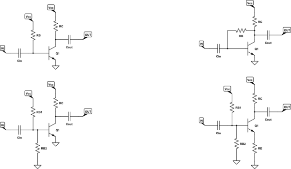
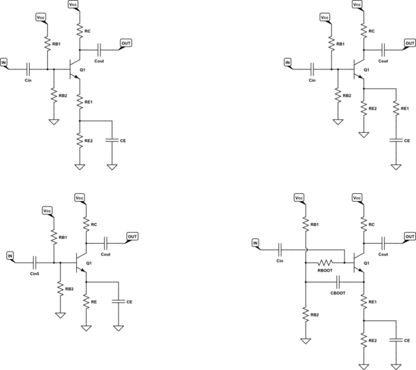
I'd like to start by throwing a bunch of slight variations on a theme. All of these below are similar BJT CE stages with similar purposes and applications. However, someday you'll want to be aware of some of the differences between them. For now, I just want to toss them out so that you won't be surprised by any of them.
schematic

simulate this circuit – Schematic created using CircuitLab
schematic

simulate this circuit

All of the above are single-ended and AC-coupled. Some exhibit highly variable gain and some don't, some are highly sensitive to ambient temperature and some aren't, some have much higher input impedance and some have much lower input impedance, some provide more degrees of design freedom and some less so. So there are various reasons for these.

I've neglected many of the incarnations that were found when germanium BJTs were more common (they have their own problems.) And I've removed some of the circuit incarnations that include modest isolation from the supply rails or where a real designer actually worked to properly shape the response of the amplifier over frequency. Trying to catalog every possible incarnation would be impossible here, anyway. But once you get a few basic variations on the theme down, they will all look similar to you and you'll immediately recognize "why this, not that" among them for any particular circumstance.

Also, many of the problems of some of the above can be repaired through something called global NFB (global negative feedback.) This is yet another concept you'll need in order to understand systems that include multiple stages chained together, for example. But that's for a later time, I think.

Let's move on.

Cononical BJT CE Amplifier Stage

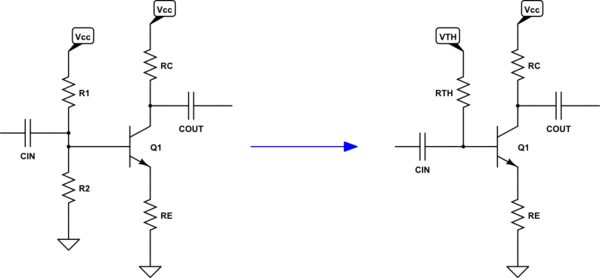
The following left-side schematic is the standard BJT CE amplifier form. On the right is the Thenenized form of the exact same circuit.
schematic

simulate this circuit

An advantage arrives because a resistor divider pair allows the added freedom of constructing a custom Thevenin voltage without needing to create another power supply rail. It always comes with a cost -- the Thevenin source resistance. But that's also under control because you can change the two base-pair resistors to whatever you want. So it's pretty nice.

The result is the right-hand schematic above. Which has a designed Thevenin voltage supply and a Thevenin source resistance. The point is the same -- biasing the BJT. But you have one additional degree of freedom now -- the Thevenin voltage -- which you wouldn't have if you just tied a resistor to \$V_\text{CC}\$ (which isn't adjustable as it is the main power supply rail.)

What Nodes to Analyze?

In the above right-side schematic there are three unknown nodes. The base, the emitter, and the collector.

You can simplify your worries a lot, though.

  • Assuming the BJT is operating in active mode (the collector has a higher voltage than the base), which is always the case for a wel-designed CE amplifier stage, the collector "looks like" a current source (infinite output impedance) and can be ignored when analyzing the circuit.
  • The base and emitter voltages are separated by just one diode drop (roughly speaking) and therefore analyzing one of them analyzes the other one.

So you really only need to solve the base voltage (or the emitter voltage) to get the other voltage.

This means it's not all that hard. You can use KVL:

$$V_\text{TH}-I_B\cdot R_\text{TH}-V_\text{BE} - I_E\cdot R_\text{E} = 0\:\text{V}$$

Since \$I_E=\left(\beta+1\right)I_B\$ it follows that:

$$I_B=\frac{V_\text{TH}-V_\text{BE}}{R_\text{TH}+\left(\beta+1\right)R_\text{E}}$$

And with that in hand it also then follows that:

$$\begin{align*}V_B&=V_\text{TH}-I_B\cdot R_\text{TH}\\\\V_E&=V_B-V_\text{BE}\end{align*}$$

Knowing \$V_E\$ allows you to now compute \$I_E=\frac{V_E}{R_\text{E}}\$ and \$I_C=\frac{\beta}{\beta+1}I_E\$. Knowing \$I_C\$ allows you to work out the voltage drop across \$R_\text{C}\$ and therefore now the collector voltage.

So that's really all there is to it. However, an assumption into all this is an a priori assumption about the value of \$V_\text{BE}\$. This value actually depends upon the value of \$I_C\$. So once you compute \$I_C\$ you can then refine the value of \$V_\text{BE}\$ and re-compute everything. Do that a few times (iterate) and you've gotten close enough.

There is a closed solution approach using the LambertW (product-log) function. But we can avoid messing with that, for now. Just iterate and you'll be good enough for most uses.

In case you want it, the Shockley equation for the active mode BJT is:

$$I_C=I_\text{SAT}\left(\exp\left[\frac{V_\text{BE}}{\eta\, V_T}\right]-1\right)$$

Or, for iterative purposes, just compute \$I_C\$ from above (not the Shockley equation immediately above, but I mean by applying \$\beta\$ to your calculated \$I_B\$ above) and then re-compute \$V_\text{BE}\$ from this:

$$V_\text{BE}=\eta\, V_T\,\ln \left(1+\frac{I_C}{I_\text{SAT}}\right)$$

Then go re-compute \$I_C\$ and repeat the process until satisfied.

The value of \$\eta\$ is usually just 1 for small-signal BJTs that are usually used in BJT CE amplifiers like this one. (It's the emission co-efficient.) The value of \$V_T\$ (the thermal voltage) is usually taken to be \$26\:\text{mV}\$ (near room temperature.) And the value of \$I_\text{SAT}\$ is something you'll need to look up for the BJT. But as a rough estimate you could use something like \$2\times 10^{-14}\:\text{A}\$ and probably be okay.
\$\endgroup\$
3
  • \$\begingroup\$ Woaw, this is really complete and clear, thank you for the explanation. I just have a last question: when you thevenize the CE amplifier, you take the Thevenin equivalent circuit of the voltage divider as seen between the base and the ground, as you would connect the load in parallel with R2. (and I agree it works well). Is it possible to take the Thevenin equivalent circuit as seen between the base and the VCC rail, as if we would connect the load in parallel with R1? Would it works and give the same result? And what would look like the thevenized circuit in this case? Thank you. \$\endgroup\$
    – wbs2422
    Commented Aug 11, 2020 at 15:43
  • 2
    \$\begingroup\$ @Wheatley You can Thevenize a single-ended wire to any voltage rail you want. It's just a different reference point. So the resistance would be the same, but the voltage would be different (probably.) And it would be referred to a different rail. But it's all the same thing. \$\endgroup\$
    – jonk
    Commented Aug 11, 2020 at 17:44
  • \$\begingroup\$ I get it, thank you very much for your explanations. \$\endgroup\$
    – wbs2422
    Commented Aug 11, 2020 at 17:48

Your Answer

By clicking “Post Your Answer”, you agree to our terms of service and acknowledge you have read our privacy policy.

Not the answer you're looking for? Browse other questions tagged or ask your own question.