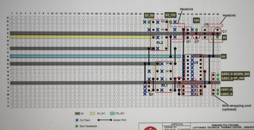
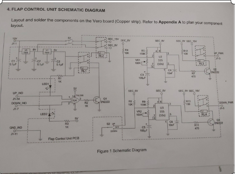
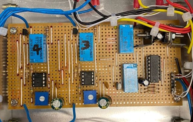
I'm new to electronics and I'm required to solder the circuit (2nd picture) onto a veroboard. I am however having trouble in designing it, with reference to the 1st picture, the left side of the circuit is already displayed on the veroboard, and I'm supposed to design the right side of the circuit and paste it on the veroboard. I dont know how to even approach this and where to put the components in the best position. The 1st picture shows shaded rows representing the 0V, 8V and 15V power lines. Can somebody guide me in completing the circuit? I have tried many times on a piece of paper but am not confident


-
1\$\begingroup\$ Welcome to EE.SE, but please crop and rotate your images and upload again. \$\endgroup\$– TransistorCommented Oct 31, 2020 at 8:42
-
\$\begingroup\$ Have updated the pictures \$\endgroup\$– BeatriceIKCommented Oct 31, 2020 at 8:49
-
1\$\begingroup\$ There is no 'best' way to lay out components on veroboard. There are several general strategies of (a) cramming everything as small as possible or (b) having all the ICs the same way up (c) making it look like the schematic (d) many other considerations. It's a PITA to do on paper. There are several CAD tools with a veroboard output, which will keep track of connectivity for you while you concentrate on aesthetics, I think Fritzing has that capability. I hope other commenters will leave suggestions for other tools. \$\endgroup\$– Neil_UKCommented Oct 31, 2020 at 8:59
-
\$\begingroup\$ Another thing I have a problem with is the pin layout of the RL components(Relay), I know it has 8 pins but am not sure which corresponds to what \$\endgroup\$– BeatriceIKCommented Oct 31, 2020 at 9:04
-
\$\begingroup\$ Check the datasheet of the relays to identify the pins. What is the part number of the relay ? If there is no part number, perhaps you can check resistance between terminals to see what is connected to what. \$\endgroup\$– AJNCommented Oct 31, 2020 at 9:13
1 Answer
That circuit is reasonably complex as it has discrete components, ICs, transistors and relays. My general approach would be
- Reserve a track at the bottom for GND.
- Reserve two tracks at the top for the +8V and +15V busses.
- You can draw a coloured lines across the top of the board to mark the busses. e.g. Black for 0V, red for 15V and blue for 8V. It can be a good idea to mark every fifth line on top and bottom so that you have some references when you invert the board.
- Lay out components in general with negative terminals towards the bottom.
- Can any components be connected directly to the negative or positive rails? In your case all three transistors' emitters can be connected to the ground rail so they can be mounted at the bottom edge of the board.
- Look for any components that can be aligned so that they can be connected as required without cutting traces.
- When you run out of easy options then you have to start cutting traces and adding jumper wires. When adding jumpers you have two design choices:
- Run wires from point to point.
- Only allow vertical links (as shown in your diagram) and use tracks for horizontal links.
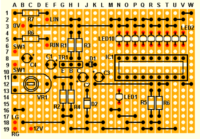
Figure 1. A tidy layout. Source: PCB Design SDL.
In the example above we can see that the designer has succeeded in keeping all the links perpendicular to the tracks. Notice all the track cuts under the LEDs, IC1, R1, R3, etc. See my answer to this question for more ideas.
Take your pick from online+stripboard+designer and start laying out.
-
\$\begingroup\$ Will take into account the advice, thanks. Just added a picture of an example completed circuit though, perhaps you can help me in my confusion on why pins 4 and 5 of the left IC is along the 0V(GND) line (Row T)? \$\endgroup\$ Commented Oct 31, 2020 at 9:31

