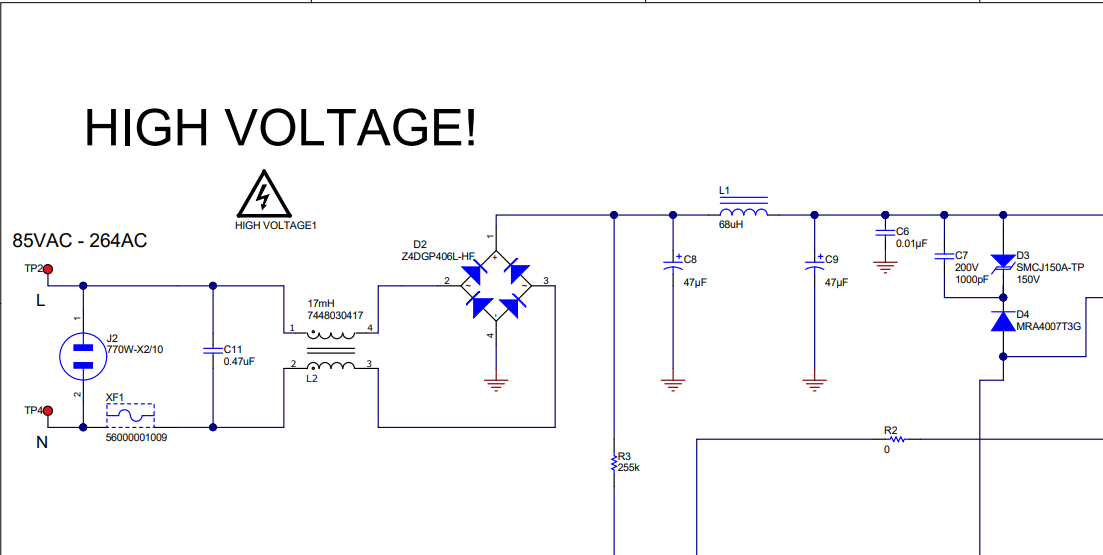
Can anyone explain why the two capacitors (C8, C9) in the CLC input
filter are set up the way that they are?
The bulk capacitance (for the reduction of AC ripple) is, in effect both C8 and C9 in parallel = 94 μF. That's fundamentally the most important role they play and, in that respect, the 68 μH is incidental at these low frequencies. It might as well be a short circuit (about 0.05 Ω reactive).
Regards higher frequencies i.e. the switching noise produced by the SMPS, the inductor (L1) plays a significant role. As has been mentioned in comments, the cut-off frequency for the \$\pi\$-filter that it forms with C8 and C9 is 3981 Hz and, above that, the filter will attenuate frequencies in either direction. So, according to the source document, the switching frequency is 100 kHz and that means that switching artefacts will be reduced by about 56.2 dB due to the effect of the \$\pi\$-filter. So now the inductor is playing a vital role in cutting down the conducted emissions caused by the switching process.
A rule of thumb of 2 - 3uF per watt of input power yields a value of
135uF - 405uF for Cin.
That might be (not sure about this) a rule of thumb for conventional (linear) transformer/rectifier/capacitor power supplies but it doesn't cut-the-mustard on an SMPS because the chip that controls the thing is capable of running down to much lower input voltages whilst still supplying a regulated output.
One more thing to consider is that the smaller the bulk capacitors are (within operational reasons), the easier it is to acquire certification in terms of its power factor; big bulk capacitors do a great job of holding-up the DC bus voltage but do a terrible job with regards to the load current profile of the switcher from the AC terminals. In effect, big bulk value capacitors do not allow a design to meet modern power factor standards.
I'm not saying the TI design does meet these standards because I don't have access to the full tear-down of the design however, I have a suspicion that it does.

