1
\$\begingroup\$

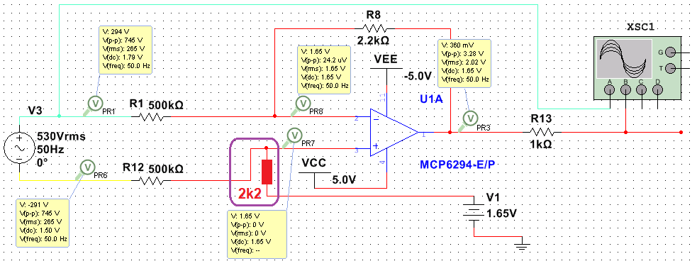
I am trying to understand the circuit have shown below. As far as I tried, it seems a differential amplifier for me. So, I tried to solve it in the way we deal with DC signals. But I failed to solve it. I couldn't understand the behaviour of this circuit. I am not good at AC signal analysis. So, I came here for help.

enter image description here

This is the circuit I am dealing with. I need to know some info about this circuit.

  1. Which kind of category this circuit belongs? I guess it belongs to differential amplifier type.Is it right?

  2. There is a voltage offset added at non-inverting input of the op-amp. If I remove this offset, the simulator shows simulation error. What's the purpose of this DC input there?

  3. This is the output signal of the circuit. Blue color denotes input, red color denotes output. Can I get the same output without adding DC offset?

enter image description here

\$\endgroup\$

2 Answers 2

3
\$\begingroup\$

Which kind of category this circuit belongs? I guess it belongs to differential amplifier type. Is it right?

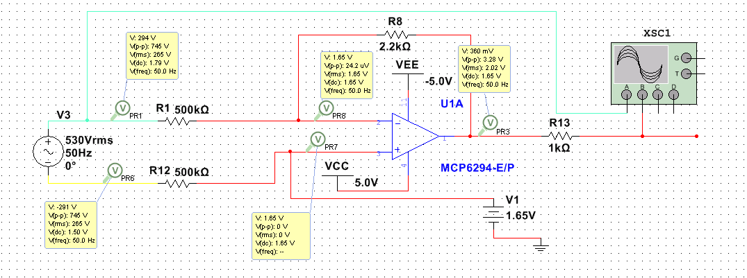
No, it's a single-ended amplifier because it doesn't have the all important extra resistor that would connect the non-inverting input with the 1.65 volt DC supply rail. See added resistor in red below: -

enter image description here

That added resistor would make it a proper differential amplifier.

There is a voltage offset added at non-inverting input of the op-amp. If I remove this offset, the simulator shows simulation error. What's the purpose of this DC input there?

Removing the offset (as in making that offset equal to 0 volts) will slightly alter the DC output from 1.65 volts to 0 volts. However, if you just removed the supply of 1.65 volts, then the non-inverting terminal wouldn't be biased and the output wouldn't be defined.

Can I get the same output without adding DC offset?
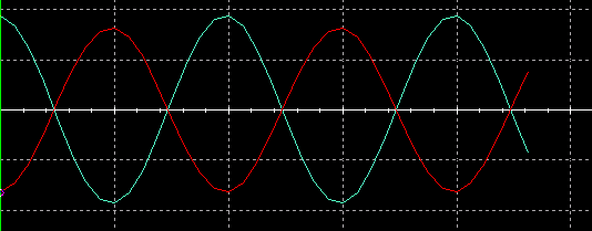
Make the DC offset 0 volts and you will get the output sinewave centred around 0 volts.

The use of two 560 kΩ resistors looks like a security measure to prevent the high voltage source (530 V RMS) from potentially injecting harmful currents into the op-amp. To understand this you'd need to consider the actual voltage source in the real circuit that the simulation is mimicking. It's likely to have several tens of pF capacitance to ground (or maybe hundreds of pF) and that leakage capacitance can form a loop that would produce excessive current into the op-amp should there not be 560 kΩ resistors present.

\$\endgroup\$
14
  • 1
    \$\begingroup\$ Thanks for your answer. \$\endgroup\$
    – CNA
    Commented Jan 19, 2021 at 11:24
  • 2
    \$\begingroup\$ Whether it is an inverting amplifier, a differential amplifier or a non-inverting amplifier, the output DC level is always dictated by the DC offset at the input @CNA \$\endgroup\$
    – Andy aka
    Commented Jan 19, 2021 at 12:21
  • 1
    \$\begingroup\$ @CNA the circuit will only work as a predictable DC voltage follower if there is no DC content in the 530 V RMS signal. Your simulation diagram shows some significant DC levels in the 530 V RMS input signal so, these can account for errors. There is also the basic offset voltage error of the op-amp to take into account. This can be a few millivolts. \$\endgroup\$
    – Andy aka
    Commented Jan 20, 2021 at 10:29
  • 1
    \$\begingroup\$ Yeah. I could see that. Also, I have found a way to calculate the output voltage Vrms with DC offset. My op amp basic offset voltage error is 0.32 mV. Thanks Andy. \$\endgroup\$
    – CNA
    Commented Jan 20, 2021 at 10:35
  • 1
    \$\begingroup\$ The amplifier will clip badly @CNA (if that is what you meant to ask?). \$\endgroup\$
    – Andy aka
    Commented Jan 21, 2021 at 13:26
2
\$\begingroup\$

Not a differential amp, because the + input of the opamp is tied to a DC voltage, not to ground via a resistor. Basically this amplifier will adjust the output voltage so that its - input remains at 1.65V DC. R1 and R12 are effectively in series so the input current is set by the input voltage going through a resistance of 1M. That same current will flow with opposite sense through the feedback resistor, and that determines the output voltage.

Essentially, this is an inverting amplifier with a DC offset. The numbers I leave to you as an exercise.

(By the way could you please format the title of your post as a question? e.g. "What kind of opamp circuit is this?" Thank you.)

\$\endgroup\$
4
  • 2
    \$\begingroup\$ Thanks for your answer. \$\endgroup\$
    – CNA
    Commented Jan 19, 2021 at 11:24
  • \$\begingroup\$ If so, will I get the output voltage using the inverting amplifier formula? \$\endgroup\$
    – CNA
    Commented Jan 19, 2021 at 12:00
  • \$\begingroup\$ more or less, but I'd suggest to just ask the question "what must the output voltage be to hold the difference between + and - inputs at zero". You learn more like that. \$\endgroup\$
    – danmcb
    Commented Jan 19, 2021 at 12:10
  • \$\begingroup\$ If I set an offset to 0V DC, I get 2.5mV to 2.90 mV DC and 1.16 Vrms at the output. This Vrms output value can be calculated using inverting amplifier gain. (i.e) 265Vrms x (2.2k/500k). If I set an offset to 1.65V DC, I get 1.65V DC and 2.02Vrms at the output. But couldn't get the output via calculation correctly. Why? \$\endgroup\$
    – CNA
    Commented Jan 20, 2021 at 5:09

Your Answer

By clicking “Post Your Answer”, you agree to our terms of service and acknowledge you have read our privacy policy.

Not the answer you're looking for? Browse other questions tagged or ask your own question.