1
\$\begingroup\$

I'm working on designing a guitar pedal based on the topology of an old tube amplifier I own.

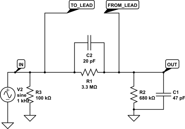
Between the amplification stages I found an inter-stage filter that I cannot understand in the frequency domain. After some research I understood that it is a capacitive voltage divider:

schematic

simulate this circuit – Schematic created using CircuitLab

I know that the filter is used for mixing some frequencies of the preceding stage (which produces the "clean", or un-distorted sound,) with the signal coming from the lead stage that is in parallel. However, for simplicity I'm focusing on the case of clean sound (lead circuit is open.)

I simulated the circuit and in this case the frequency response it is similar to that of an high-pass shelving filter, but the highs settle at about -10.5dB instead of 0dB.

Altering a single component value alters both cut-off and gain, eventually changing also the kind of filter. Indeed, I found an article stating that the transfer function of the voltage divider is:

Transfer Function

Even knowing the transfer function I cannot find out what the zeroes and poles are, since I cannot turn the equation in to.canonical form.

I need a way of expressing the two cutoff frequencies and possibly the high and low frequency gains in order to adapt the circuit to my amplitude and impedances values, while keeping the same frequency response (or even altering it in a rational way, understanding what feature is affected by each component.)

Could anyone point me in the right direction?

\$\endgroup\$
3
  • \$\begingroup\$ That's a shelf highpass, and it will give you ~5 dB between ~1 KHz and ~10 KHz. It also has very high output impedance for low frequencies (hundreds of KOhms), and a high impedance for high frequencies (KOhms). I honestly doubt you'll want this to be a filter for your amplifier, unless your input is in the GOhms range. Is this a homework? \$\endgroup\$ Commented Feb 12, 2021 at 13:58
  • \$\begingroup\$ Yes, I understand the frequency response of this particular circuit, as I already simulated it myself. What I'm asking is more related on understanding how to express the cut-off frequencies so that I can replicate the same functionality with different components, or alter the frequency response in a controlled way. As I wrote in the question, this is an actual piece of circuit from a famous tube guitar amplifier from the 70's. Since it's very popular for the sound that this way of mixing signals produce, I'd like to use the same arrangement in my guitar pedal. \$\endgroup\$
    – EdoG
    Commented Feb 12, 2021 at 14:07
  • \$\begingroup\$ Multiply numerator and denominator with (1+sR1C1). \$\endgroup\$
    – LvW
    Commented Feb 12, 2021 at 15:00

1 Answer 1

3
\$\begingroup\$

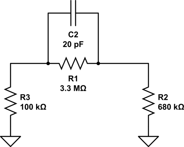
Let's analyze this circuit by inspection. We have two capacitors, meaning we expect a second order transfer function. If we're lucky, no poles are complex conjugate, so we can express the transfer function as: $$ T(s) = \frac{N(s)}{D(s)}= \alpha\frac{(1+st_L)(1+st_H)}{(1+s\tau_L)(1+s\tau_H)}$$ We can first of all derive the poles by inspection. Using a network theorem, we will derive the time constant associated with each capacitor in a superposition of effects and we will approximate the dominant pole as the sum of the two time constants. Let's start with C2.
schematic

simulate this circuit – Schematic created using CircuitLab

We get that: $$ \tau_{C_2} = C_2 (R_1 // (R_2 + R_3)) = 12.6 \mu s $$

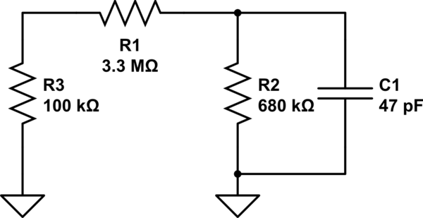
Now we do the same for C1:
schematic

simulate this circuit

$$ \tau_{C_1} = C_1 (R_2 // (R_1 + R_3)) = 26.6 \mu s $$

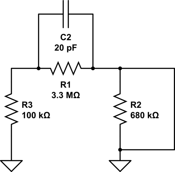
The two time constants are quite close, so the approximation we're going to do won't be great but it will give us an idea. It can be demosntrated that, if the two time constant are sufficiently far apart, the low frequency time constant of a circuit like this is: $$ \tau_L \simeq \tau_{C_1} + \tau_{C_2} = 39.2 \mu s \Rightarrow f_L = \frac{1}{2\pi \tau_L} = 4.08 kHz $$ It also holds that the reciprocal of the higher time constant is the sum of the reciprocals of the time constants calculated with the other capacitors shorted:
schematic

simulate this circuit

$$ \tau_{C_2}^\infty = C_2 (R_1 // R_3) = 2\mu s $$
schematic

simulate this circuit

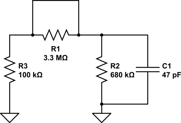
$$ \tau_{C_1}^\infty = C_1 (R_3 // R_2) = 1.7\mu s $$ So

$$ \tau_H \simeq \frac{1}{\frac{1}{\tau_{C_1}^\infty }+\frac{1}{\tau_{C_2}^\infty }} = 0.918\mu s \Rightarrow f_H = \frac{1}{2\pi \tau_H} = 173 kHz $$

Now we have both our poles, let's look for the zeros. We have a zero when, at a specific frequency, we don't have any signal at all at the output. Every capacitor introduces a zero in the transfer function and we can study them with the superposition of effects. In fact, C1 introduces a zero (allows no signal at the output) when it's a short. This means that you'll need an infinite frequency to get the zero from C1. So C1 introduces a zero at infinite frequency. Let's analyze C2. At which frequency does C2 block our signal from getting to the output? If $ C2//R1 = \infty $ we get no signal at the output. $$ \frac{1}{sC_2} // R_1 = \infty = \frac{R_1}{1+sC_2R_1} \Rightarrow 1+sR_1C_2 = 0$$ This happens for: $$ s = j\omega = -\frac{1}{R_1C_2} \Rightarrow f_z = \frac{1}{2\pi R_1C_2} = 2.4 kHz $$

Lastly, we have to consider our DC gain to calculate alpha. Basically we have a resistive divider that leads us to: $$ \alpha = \frac{R_2}{R_1+R_2} = 0.17 = -15dB $$

In the end we did get this transfer function: $$ T(s) = \alpha\frac{(1+st_L)}{(1+s\tau_L)(1+s\tau_H)}$$

So, in the audio band you will start at -15dB, then you will meet your zero at about 2.4 kHz, so your transfer function will rise at 20dB/decade until you meet your pole at about 4 kHz, then it would flatten towards infinity. Since the singularities are really close, your real transfer function will be a lot smoother than this.

Check here the bode plot of the approximation

Hope this helps.
\$\endgroup\$
3
  • 1
    \$\begingroup\$ I'm sorry that i could not find the way to insert more than one schematic, otherwise they would have been helpful \$\endgroup\$ Commented Feb 12, 2021 at 15:25
  • \$\begingroup\$ Just move further down the text and hit the schematic button again. Multiple CircuitLab schematics shouldn't be a problem at all. \$\endgroup\$
    – JRE
    Commented Feb 12, 2021 at 16:55
  • \$\begingroup\$ @JRE Thanks! I had to do one schematic per edit but i managed to do it. Some weird bugs i guess. \$\endgroup\$ Commented Feb 12, 2021 at 17:31

Your Answer

By clicking “Post Your Answer”, you agree to our terms of service and acknowledge you have read our privacy policy.

Not the answer you're looking for? Browse other questions tagged or ask your own question.