Answer
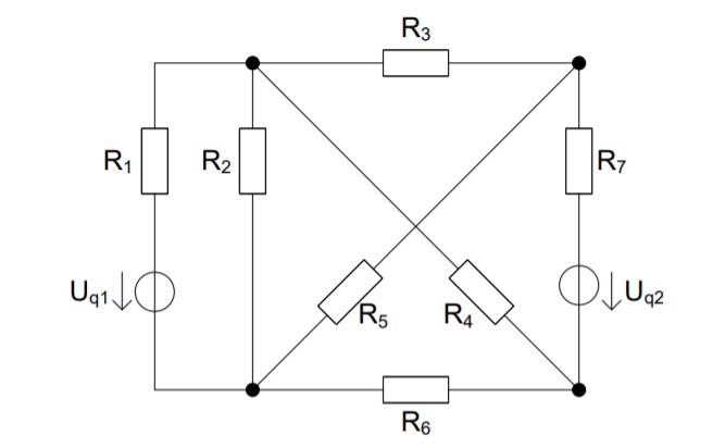
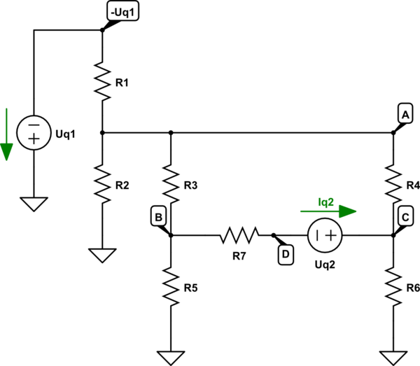
In my electrical engineering lecture we analyse such circuits with
given Resistances Ri and given Uq1 and Uq2 ( see example below ), and
we try to find the current intensity Ii at each point.
By this, I assume that \$I_i\$ is the current in each \$R_i\$. If this must also include direction (likely) then the sign will determine the direction relative to the assumed direction when writing out the equations, I suppose.
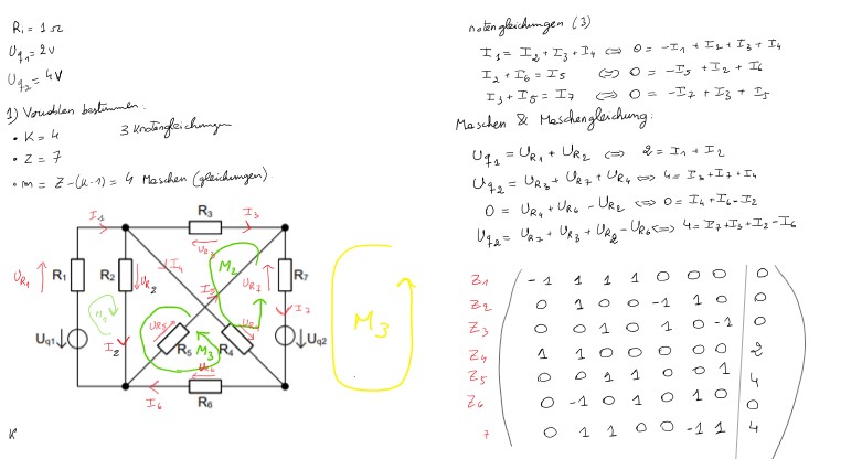
We use a long way to find them using matrices (Elimination using Gauss
process, matrice transformation, Kirchhoff laws... (see 2nd picture))
- one error can cost errors everywhere.
Yup. That's a problem and it is why I prefer to use an approach to nodal analysis that I gathered from reading Spice code. It helps avoid such difficulties. More on that, later.
1- The problem is that I can't even check if my answers are correct
when doing a exercise. Is there any tool on internet that calculates
such things ?
As already pointed out, Spice programs do this as a routine matter. If you haven't already set yourself up with some freely available Spice program, you should immediately do so.
And if you ever want to analyze a circuit symbolically rather than numerically, then you should definitely get sympy and learn to use it. You can readily solve these things using symbolic algebra, if you want.
2- Can you recommend any more secure and quicker way to analyse it ?
Thank you in advance.
Yes. And this is when I'd recommend that you learn to re-draw all schematics. Schematics are often drawn for reasons entirely apart from their readability or for simplified analysis. You need to get used to the idea that every single time you see a schematic, your first inclination should be to re-draw it for the purpose you have at hand. The only reason you should avoid it is if the schematic you are looking at is already perfect. (Which it never actually is.) See redrawing addendum below for more information.
Sometimes, it is easier to use mesh and sometimes nodal. You can often decide this by first locating unknown node voltages and name them. Also, all current sources will have an unknown voltage across them, so you'll need to create a new variable for those cases, when present. Then identify appropriate mesh loop currents for analysis, as well. Once all this is done, you can decide which is the less complex approach to take.
If you decide to go with the nodal approach, I'd very much recommend that you arrange your equations so that the outflowing currents are on the left and the inflowing currents are on the right. These must equal each other. When doing this, use the absolute values at each node. Do not attempt to make a decision about voltage differences across a component. Doing so will increase the likelihood that you'll make a mistake with respect to the sign. Using absolute values prevents you from making this kind of mistake. See the KCL Addendum below for further discussion.
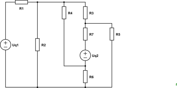
For analysis purposes, and assuming a certain meaning for your arrows with respect to the voltage sources, I'd redraw like this:

simulate this circuit – Schematic created using CircuitLab
This can now be quickly turned into the following set of nodal equations:
$$\begin{align*}
\begin{array}{c}
{\text{Node } U_A:}\vphantom{\frac{U_A}{R_1}}\\\\
{\text{Node } U_B:}\vphantom{\frac{U_A}{R_1}}\\\\
{\text{Node } U_C:}\vphantom{\frac{U_A}{R_1}}\\\\
{\text{Node } U_D:}\vphantom{\frac{U_A}{R_1}}\\\\
{\text{Equiv:}}\vphantom{U_D + U_{q_2}}
\end{array}
&&
\overbrace{
\begin{array}{r}
\frac{U_A}{R_1} + \frac{U_A}{R_2} + \frac{U_A}{R_3} + \frac{U_A}{R_4}\\\\
\frac{U_B}{R_3} + \frac{U_B}{R_5} + \frac{U_B}{R_7}\\\\
\frac{U_C}{R_4} + \frac{U_C}{R_6}\\\\
\frac{U_D}{R_7} + I_{q_2}\\\\
U_C\vphantom{U_D + U_{q_2}}
\end{array}
}^{\text{outflowing currents}}
&
\begin{array}{c}
&\quad{=}\vphantom{\frac{U_A}{R_1}}\\\\
&\quad{=}\vphantom{\frac{U_A}{R_1}}\\\\
&\quad{=}\vphantom{\frac{U_A}{R_1}}\\\\
&\quad{=}\vphantom{\frac{U_A}{R_1}}\\\\
&\quad{=}\vphantom{U_D + U_{q_2}}
\end{array}
&
\overbrace{
\begin{array}{l}
\frac{-U_{q_1}}{R_1} + \frac{0\:\text{V}}{R_2} + \frac{U_B}{R_3} + \frac{U_C}{R_4}\\\\
\frac{U_A}{R_3} + \frac{0\:\text{V}}{R_5} + \frac{U_D}{R_7}\\\\
\frac{U_A}{R_4} + \frac{0\:\text{V}}{R_6} + I_{q_2}\\\\
\frac{U_B}{R_7}\\\\
U_D + U_{q_2}
\end{array}
}^{\text{inflowing currents}}
\end{align*}$$
Using sympy:
var( 'ua ub uc ud iq2 r1 r2 r3 r4 r5 r6 r7 uq1 uq2' )
eq1 = Eq( ua/r1+ua/r2+ua/r3+ua/r4, -uq1/r1+0/r2+ub/r3+uc/r4 )
eq2 = Eq( ub/r4+ub/r5+ub/r7, ua/r3+0/r5+ud/r7 )
eq3 = Eq( uc/r4+uc/r6, ua/r4+0/r6+iq2 )
eq4 = Eq( ud/r7+iq2, ub/r7 )
eq5 = Eq( uc, ud+uq2 )
ans = solve( [eq1,eq2,eq3,eq4,eq5], [ua,ub,uc,ud,iq2] )
And from there you can generate any and all necessary values.
(If I elected the wrong polarity for your voltage sources, then adjust the above, appropriately.)
Now you have your answer regarding what tools you should acquire and learn to use.
Redrawing Schematic Addendum
Rules to live by are:
- Arrange the schematic so that conventional current appears to flow from the top towards the bottom of the schematic sheet. I like to imagine this as a kind of curtain (if you prefer a more static concept) or waterfall (if you prefer a more dynamic concept) of charges moving from the top edge down to the bottom edge. This is a kind of flow of energy that doesn't do any useful work by itself, but provides the environment for useful work to get done.
- Arrange the schematic so that signals of interest flow from the left side of the schematic to the right side. Inputs will then generally be on the left, outputs generally will be on the right.
- Do not "bus" power around. In short, if a lead of a component goes to ground or some other voltage rail, do not use a wire to connect it to other component leads that also go to the same rail/ground. Instead, simply show a node name like "Vcc" and stop. Busing power around on a schematic is almost guaranteed to make the schematic less understandable, not more. (There are times when professionals need to communicate something unique about a voltage rail bus to other professionals. So there are exceptions at times to this rule. But when trying to understand a confusing schematic, the situation isn't that one and such an argument "by professionals, to professionals" still fails here. So just don't do it.) This one takes a moment to grasp fully. There is a strong tendency to want to show all of the wires that are involved in soldering up a circuit. Resist that tendency. The idea here is that wires needed to make a circuit can be distracting. And while they may be needed to make the circuit work, they do NOT help you understand the circuit. In fact, they do the exact opposite. So remove such wires and just show connections to the rails and stop.
- Try to organize the schematic around cohesion. It is almost always possible to "tease apart" a schematic so that there are
knots of components that are tightly connected, each to another, separated then by only a few wires going to other knots. If you can find these, emphasize them by isolating the knots and focusing on drawing each one in some meaningful way, first. Don't even think about the whole schematic. Just focus on getting each cohesive section "looking right" by itself. Then add in the spare wiring or few components separating these "natural divisions" in the schematic. This will often tend to almost magically find distinct functions that are easier to understand, which then "communicate" with each other via relatively easier to understand connections between them.
- You get to choose exactly one node and call it "ground." If the purpose of redrawing the schematic is for understanding it, then choose a node that helps achieve that. When signals are single-ended, they share a common node and you should select this common node as "ground." If the purpose is for analysis, then you can select this for the purpose of reducing the equation complexity. Often, this will mean the node that is "busiest" (has the most terminals attached to it.) Either way, make this choice wisely and it will help a great deal.
The above rules aren't hard and fast. But if you struggle to follow them, you'll find that it does help a lot.
You can read a snippet of my own education by those schematic draftsmen at Tektronix who trained me by reading here.
KCL Addendum
The KCL equations may appear to treat node voltages as if they don't have to be differences, but can be absolute values. However, that's not really the case here. In fact, I'm just using superposition (which is easily seen once you've really had the concepts deepened into you.) This is, in fact, the same technique used within Spice programs (those where I've directly looked over the code used to generate these.)
Perhaps the easiest way to imagine is that absolute voltage at a node spills away from that node through the available paths. But also that absolute voltages spill into that node from surrounding nodes through those same paths. So long as you treat them all as absolute values, the result is the application of a simple superposition concept that results in, effectively, the potential differences controlling the result.
You can test this, easily, by rearranging the resulting equation(s), moving the right side over to the left side and then combining terms. You'll then see the usual potential differences that you expect. So it really is the same result.
The reason I very much prefer this method is that it is simple to visualize and very difficult to make mistakes. You can easily orient yourself to a node and then work out the terms for out-flowing currents for the left side of the equation. Then all you have to do is position yourself at each surrounding node and work out the terms for in-flowing currents for the right side. It's almost impossible to screw that up.
Conversely, when you are instead struggling to work out the potential differences in your mind (using the more traditionally taught method) and just write those terms, you often find yourself not entirely sure if you have the sign right as you try and add them up, correctly. I find, time and time again that not only others wind up messing up somewhere and making an uncaught mistake.. but that I also make those mistakes, as well. Even with lots of experience, you just aren't 100% sure and you often find yourself double and triple checking your work, just in case.
That doesn't ever happen, once you start using the superposition method. It just works. It just works right. It just works right each and every time. I've never, not once, screwed up. (I make typos. But not sign errors.) It's too easy to use.
So voltage spills away from a node via available paths and voltage spills into a node from nearby nodes via the same available paths. The only caveat is that a current source or sink can only flow in, or flow out, but not both directions. It's one way. So it will either appear on the out-flowing side or on the in-flowing side -- but not both sides.
This also works perfectly well with capacitors and inductors. It does turn the equation into a differential/integral equation. But that's just a technicality. It's still correct.

