18
\$\begingroup\$

In the circuit below, is there any reason why we can't combine R1 and R2 into one 4 kΩ resistor in either location?
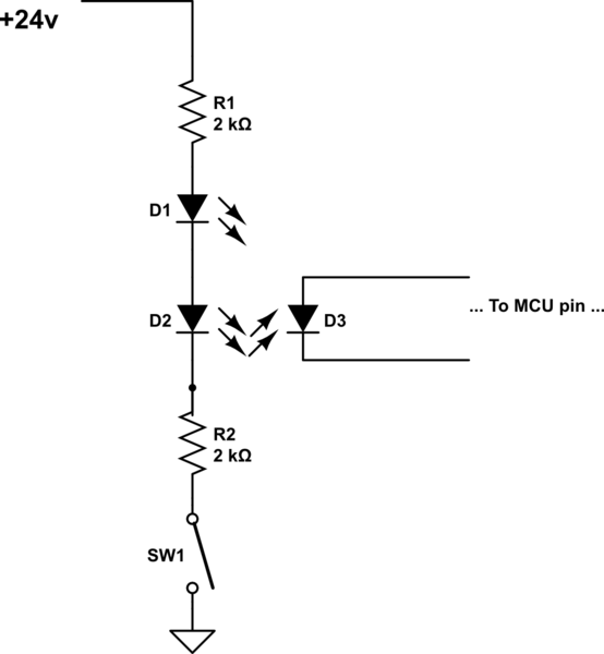
schematic

simulate this circuit – Schematic created using CircuitLab

I am reverse engineering a window controller board, which is no longer available.

The board has three input switches powered by an unregulated 24 V supply using this circuit to level-shift the inputs to the MCU's 3.3 V input pins. D2 and D3 represent an optoisolator (1/4 of LTV-846s). D1 is a visible LED that indicates when the input is pressed. R1 and R2 are 1/4 of a 8-resistor SOIC-16 SMD package (Bourns 4816P-1). Since there are three of these circuits, two of the resistors in the package are left unconnected.

Question 1: Is there any reason why this circuit would need two 2 kΩ resistors, instead of one 4 kΩ resistor? And why would they have used a SOIC-16 package for six resistors, instead of just three 0805's? The board has plenty of other discrete 0805 resistors.

I thought maybe it would be for power dissipation but unless I am making a stupid mistake, it's only dissipating 1 milliwatt which even small SMD resistors could handle.

I am going to use the same optoisolators (LTV-846s) in my new replacement board. Am I risking anything by replacing that resistor network chip with three 4 kΩ 0805 discrete resistors?

Question 2: I would be tempted to get rid of the level-shifting circuit and just use the 3.3 V supply for the switches. If the 18 AWG wires to the switch are at most 100 ft, would it be a problem to use only 3.3 V? (I think that's about 1 ohm and 1 nF in 100 ft of wire). Would I be risking activating the input, from noise picked up from the wire?

\$\endgroup\$
13
  • 8
    \$\begingroup\$ There is no reason that can be inferred from your schematic. Like Spehro said there could be some fault or failure mode to consider. But that would not be evident from the reverse engineered schematic. There is always the chance you didn't reverse engineer the schematic correctly, too. \$\endgroup\$
    – user57037
    Commented Apr 13, 2021 at 2:35
  • 10
    \$\begingroup\$ There's about 10 V across each resistor so \$ P = \frac {V^2} R = \frac {10^2}{2000} = 50 \ \mathrm {mW} \$, not 1 mW. If combined into one 4k resistor that would be 100 mW at which point it may be getting a bit warm. \$\endgroup\$
    – Transistor
    Commented Apr 13, 2021 at 7:10
  • 15
    \$\begingroup\$ On single layer boards I often use resistors to cross wires, maybe they wanted to cross twice? \$\endgroup\$
    – AndreKR
    Commented Apr 13, 2021 at 10:36
  • 12
    \$\begingroup\$ Possibly production reasons, like using 2 resistors off a reel of 4000 you already have, is cheaper than stocking one oddball larger resistor for this one product. \$\endgroup\$
    – user16324
    Commented Apr 13, 2021 at 12:29
  • 7
    \$\begingroup\$ This exercise is valuable. To me it illustrates the difference between design and development, which is when all the fun details start to matter. I agree with the answers that there is likely some external constraint, but it is not clear which one. \$\endgroup\$
    – crasic
    Commented Apr 13, 2021 at 13:48

6 Answers 6

2
\$\begingroup\$

The optoisolators serve several purposes:

  1. protecting the MCU from ESD: You'd need to design appropriate ESD protection.

  2. freeing the potential of the switches, so that if they get shorted to some other potential, no damage is done: Recall that such devices are installed by technicians who are often under a lot of pressure to get it done quickly, and mistakes that damage the controller board result in warranty claims and in general are way more pain than the cost of optocouplers. The optocouplers may even be there as a lesson learned from some previous iteration of the product that was less robust - that wouldn't surprise me.

  3. protecting the outside world from MCU's emissions: A 100ft of wire coupled to an MCU pin is a decent antenna. You'll hear the clock and the harmonics from across the street - I imagine that the MCU clock is somewhere in the 1-25MHz range, and 100ft cables are rather efficient radiators at such frequencies. With the wire coupled to the MCU pin, there'd need to be a filter network to decouple the external connection from a dirty ground and power plane.

  4. exposing an interface familiar from older product generations: It's possible that a previous generation of the product used a 24V control supply and relays to implement the control functions. The installer workforce was familiar with the voltages expected, and changes could lead to confusion, support calls, etc. It doesn't take much support line time to erase any savings from omitting the optos.

  5. providing a backward-compatible interface: It's not unthinkable that someone somewhere had a product, or a cobbled solution, that expected the inputs to survive , say, negative 24VDC. It's not clear where the long wires go, but if the wires are directly attached between the switch and the rest of the circuit, then you could for example put 24VAC at that top side of the switch, and trigger the opto.

I'd say that given the cost-to-benefit ratio, the optoisolators are the cheapest means of implementing lots of functionality while also providing lots of peace of mind. I'd also add a reverse voltage protection diode - 1N4007 backwards across the series-connected D1-D2, so that the reverse voltage seen by the LEDs is always clamped.

\$\endgroup\$
4
  • \$\begingroup\$ If there is a long wire between the LEDs and whatever is driving them, having a resistor on just one side or the other of the source would cause greater EMI emissions than putting equal resistors on both. It may also be desirable to split the resistance three ways: one on each side of the source, and one in series with the LEDs at the destination (doesn't matter precisely where, if the destination is compact). \$\endgroup\$
    – supercat
    Commented Apr 13, 2021 at 17:28
  • \$\begingroup\$ I think that is the first suggestion that gives a circuit functionality reason for splitting the resistors. Is that because the capacitance in the long wire would allow a faster rise/fall time if its before the resistor? It's not whats going on in this case because the 24v supply, LED, opto diode, and two resistors are all close together on the board. BTW, that also means that there is no possibility to short the circuit anywhere between the resistors as others have spectulated. \$\endgroup\$
    – bobjunga
    Commented Apr 13, 2021 at 20:02
  • \$\begingroup\$ You'll hear the clock and the harmonics from across the street If it's 100ft of naked hookup wire, maybe, but an appropriately shielded cable would nullify that design deficiency. \$\endgroup\$
    – J...
    Commented Apr 14, 2021 at 18:49
  • 5
    \$\begingroup\$ This doesn't seem to be answering the question at all? This is discussing the use for the optoisolator in the circuit described, but not the pair of resistors that the question is asking about. Edit: Nevermind, I see this is addressing the original "Question 2", but not question 1. I'd argue that the OP really should have asked two separate questions for improved clarity. \$\endgroup\$
    – Patronics
    Commented Apr 15, 2021 at 5:11
31
\$\begingroup\$

BOM optimization is a likely candidate. The value 2k is probably used elsewhere and adding another value would mean one more line on the BOM and one more slot in the pick-and-place machine.

Another BOM optimization could be availability. For example two 0603 resistors are easier to source than one 0805 (for power handling). You mention an eight resistor in SOIC-16. That’s certainly odd, but if you needed that special type of resistor elsewhere, you had two of the available and the layout allows it, why not use them and save a few cents?

\$\endgroup\$
1
11
\$\begingroup\$

If either side of the LED is shorted to either supply it will probably survive with two resistors. With only one, it probably won't.

If the circuit has to be resistant to "knuckleheads" perhaps the 0.1 cent for the second resistor was deemed justified.

Edit: The comment from mkeith is also very much valid. If you keep the number of different parts down it can help reduce the product cost- the number of feeders on an SMT mounting machine is limited and you may also want to avoid having to add a new part to inventory, especially if you are making less than a few thousand pieces.

\$\endgroup\$
1
  • 11
    \$\begingroup\$ Sometimes there is a desire to limit the number of unique line items in a BOM. If there were already 2k resistors on the BOM, maybe someone got the idea that it would be better to use 2 of them rather than introduce a new line item for 3.9k. \$\endgroup\$
    – user57037
    Commented Apr 13, 2021 at 4:32
5
\$\begingroup\$

Is there any reason why this circuit would need two 2k resistors instead of one 4k resistor?

No.

I thought maybe it would be for power dissipation but unless I am making a stupid mistake, its only dissipating 1 milliwatt which even small SMD resistors could handle.

Subtract the voltage drop of two LEDs from 24V. To be conservative let's say 20V. 20V/4k\$\Omega\$ is 5mA. 5mA times the 20V gives 100 mW.

I would be tempted to get rid of the level shifting circuit and just use the 3.3v supply for the switches.

Although it is not clear how the ground is related to the +24V, I would guess that the circuit is basically "current loop". Current loop has a high immunity to induced voltages. If you connect your switch to the MCU directly through a 100 foot cable, (you would also need a pull-up or pull-down resistor) it will be the voltage at your pin that is important. Your noise immunity will be gone. Additionally, you risk damaging the input pin of your MCU (or more) if there are induced voltages that bring the pin beyond its rated voltage. I would stick with opto-isolation.

Would I be rising activating the input from noise picked up from the the wire?

Use twisted pair, to minimize noise from the long length of wire. Any cable rated for RS422 or RS485 should be fine. If you happen to have spare ethernet cable, that will work also, but has more conductors than you need. Even telephone cabling should be fine.

\$\endgroup\$
2
  • 1
    \$\begingroup\$ This is what I thought, but it worries me (a little) to change the design without understanding why it was done this way in the first place (maybe they had some 4816P-1 chips laying around that they needed to get rid:). I am going to leave the question open for a while to see if anyone can calm my nerves by offering a reason why. \$\endgroup\$
    – bobjunga
    Commented Apr 13, 2021 at 2:12
  • \$\begingroup\$ A detailed article on protecting your inputs when using long wires: digikey.com/en/articles/… \$\endgroup\$ Commented Apr 13, 2021 at 16:17
4
\$\begingroup\$

The resistors are split for better common-mode transient immunity (CMTI), i.e. for better separation of the two supply domains. The two sides are galvanically isolated, otherwise there would be no reason to use optodiodes (=isolators).

If there is any noise (more like disturbances caused by motors, or high current fast circuitry) on one of the supplies, then it will galvanically couple to the other side through the capacitances between the two supply domains. In the following analysis I will assume that there is one equivalent capacitor from the secondary side to both the anode and the cathode of the optodiode. The optocoupler itself have such parasitic capacitors as well. Basically the problem is that the current through such a capacitor can turn on the optodiode, or it can steal current from it. Both of the cases lead to an erroneous signal.

The goal is to keep the current through the optodiode the same, regardless of ground bounce, or noise between the supplies. The optodiode can be thought of as a short when it emits light, and an open, when it does not. The ratio of the two resistors should match the ratio of the capacitors.

If the diode is turned off, the voltage drop on the two resistors should be the same in order to keep the diode turned off. Therefore $$ \frac{dV}{dt} C_1 R_1 = \frac {dV}{dt}C_2 R_2$$

If the diode is turned on, then the "noise" current through it from the two capacitance should cancel each other, i.e. $$ \frac{dV}{dt}C_1 \frac {R_1} {R_1 + R_2} = \frac {dV}{dt} C_2 \frac {R_2} {R_1 + R_2} $$

Note that this analysis is simplified, because it assumed that there is only one node from the other side with coupling capacitors, but in most of the cases it is fairly accurate.

You should know or at least have a guess whether CMTI is something you have to care for. Check the datasheet and application notes from the optocoupler supplier for information about the capacitance ratio. Even if it is not critical, it makes sense to split the resistors, to reduce this effects. This 1:1 split is probably something like that.

Also you should consider BOM simplification, which could save you some time to find the right resistor if you build a new one (or save a feeder and manufacturing setup, plus logistics).

This and this application notes seem to be a good starting point for reading about it. I remember an even better one, but I was not able to found it now.

I also would like to note for completeness, that optical isolation is kind of an old technology now. Even though there are efforts to increase its robustness and lifetime, there are other chip sized solutions. Probably capacitive isolation barriers are the best for price per performance ratio. These chips might have digital in- and output, integrated gate drive, or even secondary side DCDC controllers. All of these make the life of a designer easier.

\$\endgroup\$
2
  • \$\begingroup\$ It sounds credible, but do you have a source for the first claim? \$\endgroup\$ Commented Apr 15, 2021 at 13:37
  • \$\begingroup\$ @PeterMortensen It has to be described in the two linked document. I've written my answer from memory. I've been involved in the developement of such an optoisolator few years before, and this was the big deal: get as good CMTI as possible for as low power consumption as possible for as high yield as possible on a cost efficient technology. \$\endgroup\$ Commented Apr 15, 2021 at 14:00
1
\$\begingroup\$

I did this exact thing in a design for heat dissipation. But, my design didn't have a fixed voltage as input like yours, rather it had a wide input range.

\$\endgroup\$

Your Answer

By clicking “Post Your Answer”, you agree to our terms of service and acknowledge you have read our privacy policy.

Not the answer you're looking for? Browse other questions tagged or ask your own question.