0
\$\begingroup\$

I want to make an MCU operated buck converter with the lowest operating current possible since most electronic shops near me only offered buck converters with an operating current of 10 mA and above. To achieve that, I've come up with the design below for the MOSFET gate driver, however, some questions came into my mind when I placed the R1 resistor to limit the base current (I want to reduce current draw as much as possible since I will be relying on batteries to power this project); in the discharge phase (Q1 and Q3 ON, Q2 OFF) the peak saturation current for the Q1 transistor will shoot up for a moment because of the added current of the discharge from Q3, will the limited Ib prevent the discharge from happening as planned? Or in other words, should I account for the discharge current when I'm calculating the value of IBQ1(sat) and R1? I do realize that increasing the value of R2 to avoid losses will greatly affect the Ton time of the MOSFET since the gate drive current is decreased (unless I use a Darlington pair or a BJT with high enough current gain which might have a poor frequency response) but that shouldn't be a problem since I will be satisfied with a turn on delay of 0.09 µs.
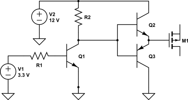
schematic

simulate this circuit – Schematic created using CircuitLab

Important Specs: PWM frequency from the MCU: 500 kHz (it has to be from the MCU because the stm32 that I'm using is very good at generating PWM without consuming much power). MOSFET total gate charge: 63 nC. Total maximum average current draw should be <10 mA (as low as possible). MOSFET used: IRF5305.

Notes :- I also did not find any reasonably priced MOSFET gate drivers which is why I decided making my own.

  • the buck converter will only be running for a about ten seconds to power the MCU when it is awake and two servo motors with a total maximum draw of 0.34 A, the buck converter will be turned off once the MCU returns to sleep-mode.

Even if this design might not be suitable for this application, it would be very helpful if you could answer the questions above, if you had other concerns regarding the circuit feel free to share them aswell.

\$\endgroup\$
14
  • 1
    \$\begingroup\$ The important is R2 affects turn on time of Q2 (so turning off of M1) and even gate voltage when M1 is off. It is becouse with this push-pull driver you will never pull gate to 12V. There will be always drop between 12V and gate about Vbe_Q2+R2*Ib_Q2 so you can see how this drop rises when you use a huge R2. \$\endgroup\$
    – user208862
    Commented Aug 29, 2021 at 23:59
  • 1
    \$\begingroup\$ Start with 1st principles of Ic=CdV/dt and specs for ramp up time and V tolerance error and load R + C. 10 mA is tight for buck considering the charge current to ramp up and supply decoupling needed \$\endgroup\$
    – D.A.S.
    Commented Aug 30, 2021 at 0:06
  • 1
    \$\begingroup\$ Ok, consider Q1 is turning off slowly because off huge R1 (discharging its junction). This couses slow turning on of Q2 and also slow M1 off transition so R1 add a huge delay and I doubt you will reach 500kHz with high-ohm resistors. Advantage is if you gonna hold converter off most of the time the resistors will drain almost nothing with this topology (no current flow when 3v3 is off) so there is no reason to use high resistances. \$\endgroup\$
    – user208862
    Commented Aug 30, 2021 at 0:18
  • 1
    \$\begingroup\$ @A.H.Z List out your key requirements for your application. A blinkered (narrow) focus on this stage, which is merely one part of something much larger, will cause you to lose sight of the actual goals. So you need to start with the overall system design requirements and then, incrementally and painstakingly, break them down into section requirements. I don't think that's been done so I don't think you are in a position to provide appropriate specifications for this section, yet. But whatever they are, they will most certainly include details derived from the driven FET load requirements. \$\endgroup\$
    – jonk
    Commented Aug 30, 2021 at 0:32
  • 1
    \$\begingroup\$ No sol'n is in sight without reasonable energy limits you must impose in your ? along with a list of tolerances. E=1/2 CV^2+VI*t. Efficiency, error, and ripple tolerance. Consider the Q of the switch and excess reactive energy and losses of same considering the short operation. \$\endgroup\$
    – D.A.S.
    Commented Aug 30, 2021 at 2:24

1 Answer 1

2
\$\begingroup\$

"I want to make an MCU operated buck converter with the lowest operating current possible since most electronic shops near me only offered buck converters with an operating current of 10 mA and above."

Here is a part that can be used, lower quiescent current. https://www.befr.ebay.be/itm/234047609405?hash=item367e531a3d:g:B6kAAOSwI8Jg0Neo

MPM3610 FEATURES

  • 4.5V to 21V Operating Input Range

  • 1.2A Continuous Load Current

  • 200μA Low Quiescent Current

\$\endgroup\$
1
  • \$\begingroup\$ I will definetly check it out. \$\endgroup\$
    – A.H.Z
    Commented Aug 30, 2021 at 16:46

Your Answer

By clicking “Post Your Answer”, you agree to our terms of service and acknowledge you have read our privacy policy.

Not the answer you're looking for? Browse other questions tagged or ask your own question.