0
\$\begingroup\$

enter image description here

Reference: Device Electronics for Integrated Circuits 3rd Ed. Richard Muller

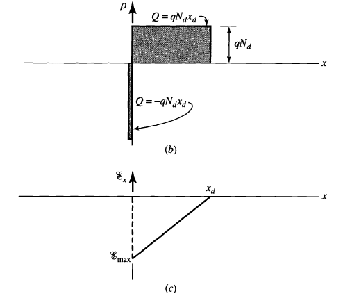
I am trying to understand how to calculate the maximum electric field. The answer given in the book is $$E_{max} = \frac{-q N_d x_d}{\epsilon_s}$$ But I am not so sure how to determine the maximum electric field based on the charge distribution alone. Here is what I tried. Using the Gauss's law, $$\int_{0}^{x}dE = \int_{0}^{x}\frac{\rho}{\epsilon_s}$$ $$ E(x) - E(0) = \frac{\rho}{\epsilon_s}x $$ $$ E(x) = \frac{\rho}{\epsilon_s}x + E(0) = \frac{q N_d x}{\epsilon_s} + E(0) $$

From here, since I know the electric field should be zero at the boundary of the depletion region (x_d), I concluded that $$ E(0) = \frac{-q N_d x_d}{\epsilon_s} $$

But this feels like cheating and I feel that I should be able to calculate the electric field at x = 0 without making the use of the knowledge that the electric field outside of the depletion region is zero.

I also tried calculating the electric field due to the sheet charge, assuming an infinite plane, $$ E_{sheet} = \frac{\sigma}{2 \epsilon_s} = \frac{-q N_d x_d}{2 \epsilon_s} $$ But I am not sure what to do with this.

What am I missing here?

\$\endgroup\$

1 Answer 1

1
\$\begingroup\$
  1. There is no cheating in applying depletion approximation to a metal-semiconductor junction when solving problems for which this approximation holds. Apart from that, the total electric charge of the space charge region (depletion region) is zero (see overall charge neutrality of the depletion region in the Wikipedia article on depletion region), and you can safely apply the boundary condition E(x) = 0 for x outside this region.

  2. It is true that Poisson’s equation in electrostatics is the Gauss’s law in differential form, but, when applying the integral form and calculating electric flux, one integrates over a closed surface enclosing the charge distribution. In your arrangement, you would integrate over the plane y-z. The integral over \$x\$ calculates the total charge in the region, and not the electric flux. Having the total charge calculated in this way, you can apply Gauss's law in its integral form (due to a symmetry of your 1D arrangement, you need not solve Poisson's equation). You notice that the electric field is uniform and constant for your arrangement, and apply Gauss's law to two unit squares, one of the y-z plane located at \$x\$ outside the depletion region (where the flux from semiconductor charges is \$σ/(2ϵ_s)\$), and the other one of the y-z plane located at \$x=0\$ (where the flux from semiconductor charges is \$-σ/(2ϵ_s)\$). Because the square is unit and the electric field is orthogonal to this square, the flux is numerically equal to the electric field strength, and, by force of Gauss's law, the flux is equal to the total charge under this square into the depletion region depth divided by absolute permittivity. You arrive at the textbook answer.

  3. The electric field of infinite sheet is \$σ/(2ϵ_s)\$. Because the total electric charge of the space charge region (depletion region) is zero, the total charges in both sheets are equal and opposite sign; the sheets are located on the opposite sides of the junction; therefore, the contributions of two sheets from both sides of the metallurgical junction, one semiconductor and the other metallic, sums up to \$E(0)=σ/(2ϵ_s)-(-σ/(2ϵ_s))=−qN_dx_d/ϵ_s\$.

Notice also that your slide (b) shows the total charge in metal as the opposite to the total charge in semiconductor (they use overall charge neutrality). As a function of carrier concentration and depletion depth in metal, it reads $$ Q = -qN_Mx_p $$ where \$N_M\$ is the carrier concentration in metal, \$x_p\$ is the depletion depth in metal.

We calculated the maximum field strength \$E(0)\$ with Gauss's law, substituting the total charges into formulas, without calculating the \$x_n\$ and \$x_p\$ values. To find the charge distribution, one needs to solve Poisson's equation and the material equation for pn-junction, which include two unknowns, \$x_n\$ and \$x_p\$. In the metal-semiconductor junction of Schottky diode, though, \$N_M\$ is high and so \$x_p\$ is small.

\$\endgroup\$

Your Answer

By clicking “Post Your Answer”, you agree to our terms of service and acknowledge you have read our privacy policy.

Not the answer you're looking for? Browse other questions tagged or ask your own question.