2
\$\begingroup\$

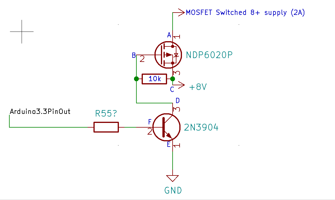
I have this schematic below. I have a circuit to switch 8 V power using a MOSFET and an NPN transistor with an Arduino's 3.3 V. The power of the switched side will be around 2 A (if this matters somehow).

Enter image description here

I have two questions.

  1. What's the value of R55? How is it calculated and is it related to the 2 A in any way?

  2. When the Arduino pin is in the LOW state, point D measures 8 V. When the Arduino pin is in HIGH state, point D measures around 0.3 V. According to my understanding, point B is always on 8 V, because it gets voltage from the battery in point C. How come that the transistor "breaks" that from point D to B and lowers/overrides that voltage coming from point C?

\$\endgroup\$
1
  • 2
    \$\begingroup\$ Please draw your schematics right-side-up. It makes it very hard to understand it when you draw it upside down. Please flip the top transistor vertically. \$\endgroup\$ Commented Nov 12, 2021 at 18:59

5 Answers 5

4
\$\begingroup\$

No wonder there's problems understanding the schematic. It's drawn in an unconventional way, the FET is upside down for extra confusion.

  1. Value of R55 is not indicated, and it would be calculated as usual for driving transistor bases. A milliamp would be a good starting point. It has no connection to any 2A currents.

  2. You have determined how point D works correctly. But please note that points D and B are the same point as they are connected by wire. The BJT transistor drives the FET gate to turn the FET on or off.

\$\endgroup\$
4
\$\begingroup\$

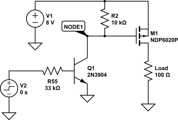
Let's rearrange. R55 does not depend on the 2A of your load at all; it is there to control the gate of the NDP6020P. If R55 is too low, you'll possibly burn out the 2N3904 by passing too much current through the B-E junction. If R55 is too high, you won't draw enough current through R2 to lower M1's Vgs enough to turn it on. In between, you have a range of options that change M1's switching speed and drive strength.

When the Arduino output to the base of Q1 is low, there is no base current so (essentially) no collector current flows and NODE1 gets pulled up to 8V by R2. When the Arduino output goes high, base current flows, which allows collector current to flow, and NODE1 drops by Ic*R2.

EDIT: included @mkeith's R55 value.

schematic

simulate this circuit – Schematic created using CircuitLab

\$\endgroup\$
4
  • \$\begingroup\$ Thanks so much ! So neglecting R55 at all, bad idea ? \$\endgroup\$ Commented Nov 12, 2021 at 19:26
  • 1
    \$\begingroup\$ Yes, you can think of the base-emitter junction of Q1 as a sort of diode. If you have nothing to limit the current through it, it is certainly capable of passing enough to damage itself. @mkeith has a good explanation of how to calculate the resistor. \$\endgroup\$
    – vir
    Commented Nov 12, 2021 at 19:28
  • \$\begingroup\$ One more question if you will, how come that the R2 resistor is not affecting the current flowing through the M1 and only affects Q1 ? \$\endgroup\$ Commented Nov 13, 2021 at 7:44
  • 1
    \$\begingroup\$ because M1 is a Field Effect Transistor, which does not have any kind of galvanic connection between its gate and the source-drain path (except for leak current and a parasitic capacitance). it is driven not with current, but with charge. \$\endgroup\$
    – dlatikay
    Commented Nov 13, 2021 at 11:35
4
\$\begingroup\$

2n3904 is being used as a switch. It controls the voltage at point B. The 10k resistor pulls point B high (to 8V) but when 2n3904 is turned "ON" then it provides a low impedance path from point B to GND. So the 10k resistor pulls point B high, but when you turn on 2n3904, it pulls point B down, and it pulls a lot harder than the resistor so it wins the tug-of-war.

R55 controls the amount of current in the base of 2n3904. You are using 2n3904 as a saturated switch, so you want the base current to be about 0.1 x the collector current (more is also OK). The collector current is 8 V / 10 k = 800 uA. So the base current should be 80 uA.

Typical base voltage in a circuit like this will be about 0.6 V.

Base current is VDD - 0.6 V / R55. So we want to set that equal to 80 uA and solve for R55.

From your schematic, VDD is 3.3 V. So:

R55 = (3.3 - 0.6) / 80 uA

R55 = 33,750 Ohms.

So you can use a 33 k resistor (33 k is a standard value). If VDD changes, or if the 10 k resistor changes, or if the switched voltage is not 8 V, then you should recalculate R55.

\$\endgroup\$
6
  • \$\begingroup\$ Amazing, thanks! Is neglecting R55 at all can damage 2n3904 in any way ? or what are the implications ? \$\endgroup\$ Commented Nov 12, 2021 at 19:25
  • 2
    \$\begingroup\$ You have a very wide range of acceptable values for R55, but it should be there to avoid excessive current in the base or 2n3904. It is possible that 2n3904 could be damaged if R55 is 0 Ohms or 100 Ohms or something like that. Anything over 1 k will probably protect it. You could substitute a low-power mosfet instead of 2n3904. For example BSS138, and in that case, 0 Ohms would be OK (R55 would not be needed). \$\endgroup\$
    – user57037
    Commented Nov 12, 2021 at 19:35
  • \$\begingroup\$ I forgot , where did the 0.6v value is coming from in your calculation ? \$\endgroup\$ Commented Nov 13, 2021 at 5:51
  • 1
    \$\begingroup\$ Oh, sorry. 0.6 V is the voltage drop from base to emitter of a typical BJT. It could be a bit higher or lower depending on ambient temperature and how much current you run through it. Usually people use 0.6 or 0.7 V for this type of calculation. \$\endgroup\$
    – user57037
    Commented Nov 13, 2021 at 6:17
  • 1
    \$\begingroup\$ Regarding the R55 being possibly omitted - it would be the Arduino's TTL output, rather than the 2N3904 base, that I'd worry about :-) Not sure if the Arduino's outputs are short-circuit-safe... otoh the general-purpose discrete BJT should survive a couple milliamps of base current. \$\endgroup\$
    – frr
    Commented Nov 13, 2021 at 7:01
2
\$\begingroup\$

What's the value of R55 , how is it calculated and is it related to the 2A in any way ?

It has no relation to the 2A of the PMOS switch. This resistor is the base resistor of the NPN BJT. The value is around 4.7 kohm, it has to pass enough base current, so that BJT goes in saturation region - operation of the transistor as a switch. If the transistor would conduct withot any loss (zero resistance) the collector current would be 8V/10kohm= 0.8mA. As we know Ic=Beta*Ib, you can calculate Ib, then the max. value of the base resistor. Beta minimum for 2n3904 is somewhere of 40, so Ib has to be >= 20uA. Rb=(3.3V-0.65V)/20uA < 133 kohm.

When the Arduino pin is in LOW state, point D measures 8V. When the Arduino pin is in HIGH state, point D measures around 0.3v.

Well, it should be more closer to 0.6V.

According to my understanding point B is always on 8v because it get's voltage from the battery in point C.

No, there is a 10k resistor in between B and C.

How come that the transistor "breaks" that from point D to B and lowers/overrides that voltage coming from point C ? I hope I got my question right here:)

Points B and D are the same.

\$\endgroup\$
2
  • \$\begingroup\$ thanks a lot !!! how did u calculate the 0.6v, actually i think i measured around 0.3v when my input was 8.2v , does it make any sense ? \$\endgroup\$ Commented Nov 13, 2021 at 5:53
  • 1
    \$\begingroup\$ @JordanSheinfeld Sorry, I have took a look into a datasheet and Vce(sat), truly is 0.3V. \$\endgroup\$ Commented Nov 13, 2021 at 10:01
1
\$\begingroup\$

These discussions are rather advanced in my opinion, as you were asking about fundamentals that i gather from your follow up questions that you have not yet understood. This is not strange att all considering that no one here seems to want to just Keep it simple, so i thought i'd give it a go. DO Keep in mind that this is quite a bit simplified;

The 10k resistor between B and C allways delivers current to node B. No matter what. But when the BJT turns on and provides a path from B to ground you can more or less view the BJT as a low-value resistor, as it has a very much lower resistance than 10kOhm This means that you now have 2 resistances in series between your 8 volts and ground. (From C to B to GND).

As you may know, 2 resistances in series between a voltage source and GND is what we call a resistive voltage divider (IF you don't know what this is you should Google it, it is a simple concept) When the resistance closest to ground is much lower than the one closest to your voltage source, the voltage between the resistances (in this case at point B) will be closer to GND (0v). And reversely if the resistance closer to the voltage source is the smaller one, then the voltage in between them would be closer to the voltage source (8v). This is what causes the voltage to drop at the MOS gate even thought current is still flowing from C to B through the 10k resistor.

And like others have pointed out earlier, a BJT base always need to be driven through a resistor as the BJT's internal resistance from base to emitter is so low you can basically call it a short circuit. What they have not pointed out though, is that while this would destroy your BJT, wich is really cheap, it would most likely also destroy your Arduino as the short circuit current through the BJT is drawn directly from your Arduino, and is much higher than the 20 or so milliamps that an Arduino pin can provide.

\$\endgroup\$
1
  • \$\begingroup\$ Thank you very much! Indeed you pointed out really good explanation of the things I appreciate that! It's even more clearer now. \$\endgroup\$ Commented Nov 15, 2021 at 18:49

Your Answer

By clicking “Post Your Answer”, you agree to our terms of service and acknowledge you have read our privacy policy.

Not the answer you're looking for? Browse other questions tagged or ask your own question.