2
\$\begingroup\$

When designing op-amps at the transistor level, the op-amp output is given by:

vout = Aol(vinp - vinm)

where vout, vinp and vinm are small signal changes in the output and input voltages.

How come that the absolute output level when analyzing op-amp circuits is assumed to be Vout = Aol(Vinp - Vinm)?

Here, Vinp and Vinm are the absolute voltage levels of the input pins, in contrast with vinp and vinm

The Op-amp is designed with both inputs at a certain bias point, Vin,cm.

vinp - vinm = (Vinp-Vin,cm)-(Vinm-Vin,cm)=Vinp - Vinm

But Vout =vout + Vout,cm where Vout,cm is the output when there is no small signal input, i.e, when the input pins are at the bias point.

Shouldn't the opamp output be Vout = Aol(Vinp - Vinm)+Vout,cm

\$\endgroup\$

4 Answers 4

3
\$\begingroup\$

Yes, that is strictly true, however usually the Vout,cm divided by Ao is so much less than the input offset voltage that it doesn't really matter.

It makes more sense to assume Vout,cm == 0 for an op-amp with equal bipolar supplies. Otherwise you might want to use midpoint between the two supply rails.

\$\endgroup\$
2
  • \$\begingroup\$ Let's say I designed an Op-Amp with Vdd = +- 1V and both inputs are normally biased at 0V. Without feedback, the output is not necessarily at 0V. In fact it can be anywhere, even up to +- 0.5V \$\endgroup\$ Commented Nov 14, 2021 at 7:11
  • \$\begingroup\$ If the Vos is +/-100uV and gain is 10^6 then the output can certainly be anything within the output swing capabilities. So if you assume 0 or 0.5V or 1V it makes little difference to the calculations. \$\endgroup\$ Commented Nov 14, 2021 at 7:15
2
\$\begingroup\$

The output of an ideal op-amp is given by

$$V_{out} = A_{ol}(V_{in+}-V_{in-})$$

Using this ideal model of an op-amp, we can fairly accurately predict the closed loop behavior of an op-amp circuit containing negative feedback.

However, this ideal op-amp is a useful fiction. Real op-amps do not have that behavior. A real op-amp acts more like an integrator than a strictly proportional amplifier. This integration comes about from the compensation capacitor in the op-amp, and reduces the error, when there is negative feedback, to near zero.

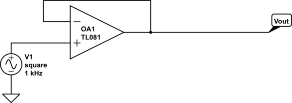
The following circuit illustrates.

schematic

simulate this circuit – Schematic created using CircuitLab

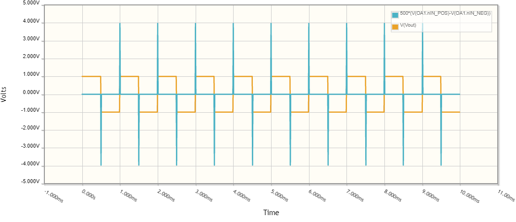
I have run a simulation of this circuit and plotted the error voltage, i.e. \$(V_{in+}-V_{in-})\$ together with the output. One can easily see that the error voltage consists of alternating spikes and the output is the integral of these alternating spikes. (The error voltage is scaled by a factor of 500 so that it fits nicesly in the same plot as the output.)

enter image description here

Note that the output of this circuit (a voltage follower) nicely tracks the (non-inverting) input, just as if it obeyed the equation

$$V_{out} = A_{ol}(V_{in+}-V_{in-})$$

But it clearly does not obey that equation. The moral? The model of the ideal op-amp gives very good results for modeling op-amp circuits with negative feedback. However, that model does not accurate represent what is really happening in an op-amp.

\$\endgroup\$
2
\$\begingroup\$

How come that the absolute output level when analyzing op-amp circuits is assumed to be \$V_{out} = Aol(V_{inp} - V_{inm})\$?

Simply put, it is not. No-one in the industry assumes this \$V_{OUT} = Aol(V_{inp} - V_{inm})\$ to be true or even useful for analyses embracing common mode parameters as is the case of your \$V_{IN,CM}\$ and \$V_{OUT,CM}\$.

But you are right, the handling of opamp's VTC in the presence of non-negligible common mode signal gain should be taken with special care: you should be familiar with the terminology, be able to read the relevant sections of datasheets, and trace the issues of input/output common-mode ranges violation and output latchup in your designs.

A good starting point to learn about common-mode issues might be Analog Devices' tutorials. MT-042 introduces the notion of Common-Mode Rejection Ratio:

If a signal is applied equally to both inputs of an op amp, so that the differential input voltage is unaffected, the output should not be affected. In practice, changes in common mode voltage will produce changes in output. The op amp common-mode rejection ratio (CMRR) is the ratio of the common-mode gain to differential-mode gain.

INLINE COMMENT


When citing their CMRR definition, I noticed that the MT-042 definition of CMRR (the ratio of the common-mode gain to differential-mode gain) is at odds with the generally accepted one (The CMRR is defined as the ratio of the powers of the differential gain over the common-mode gain). Evidently, this is a typo, because further on, the CMRR value they use in the text and formulas, is the ratio of the differential-mode gain to common-mode gain, the inverse value w.r.t. their wording. Analog Devices, please correct this typo!


Back to the answer. Pay attention to formulas in Fig. 2: Calculating Offset Error Due to Common-Mode Rejection Ratio (CMRR) of this tutorial:

$$ \text {ERROR (RTI)} = {\frac {V_{CM}} {\text{CMRR}}} \\ V_{OUT} = \left[1+{R2 \over R1}\right] \left[V_{IN}+{\frac {V_{CM}} {\text{CMRR}}}\right]\\ \text {ERROR (RTO)} = \left[1+{R2 \over R1}\right]{\frac {V_{CM}} {\text{CMRR}}} $$

These are the formulas for a closed-loop configuration. Listed in datasheets, the parameters CMRR and CMR characterize the rejection of a common-mode signal component in the total output of opamp.

The middle formula is valid for the approximation of \$R2/R1 \ll Aol\$. For \${1 \over R2} = 0\$ (no feedback, open-loop configuration), it should be written (https://en.wikipedia.org/wiki/Open-loop_gain, section Role in non-ideal gain) $$ V_{OUT} = Aol \left[V_{IN}+{\frac {V_{CM}} {\text{CMRR}}}\right] = Aol \left[V_{IN}+{\frac {Acm} {Aol}}V_{CM}\right] = Aol·V_{IN} + Acm·V_{CM} $$ because \${\text{CMRR}} = {\frac {Aol} {Acm}}\$ by definition. Also by definition, \$Acm·V_{CM} = V_{OUT,CM}\$, and \$V_{CM}\$ is a common-mode voltage at the input, \$V_{IN,CM}\$. In the end, we arrive at your formula \$Vout = Aol(V_{in+} - V_{in-})+V_{OUT,CM}\$.

Also pay attention to this phrase in the first paragraph

please note that there is very little consistency in this throughout the semiconductor industry with regards to the use of dB or ratio values for CMR or CMRR.

which emphasizes the importance of following the terminology.

MT-041 considers practical basic points regarding the allowable input and output voltage ranges of a real op amp. These obviously vary with not only the specific device, but also the supply voltage.

To grasp a deeper understanding of CMRR, follow also tutorials and datasheets referenced in these two tutorials, as well as app notes, handbooks and tutorials of the other opamp manufacturers (Texas Instruments, STMicroelectronics), textbooks and EE course notes.

\$\endgroup\$
1
\$\begingroup\$

The output an amplifier is equal to the differential input multiplied by the differential gain plus the common mode input multiplied by the common mode gain.

The differential input is the difference between the inputs and the common mode input is the average of the two inputs.

The common mode rejection ratio is equal to the differential gain divided by the common mode gain which is usually a very large number.

When the common mode rejection ratio is specified in dBs it is referred to as common mode rejection.

\$\endgroup\$

Your Answer

By clicking “Post Your Answer”, you agree to our terms of service and acknowledge you have read our privacy policy.

Not the answer you're looking for? Browse other questions tagged or ask your own question.