0
\$\begingroup\$

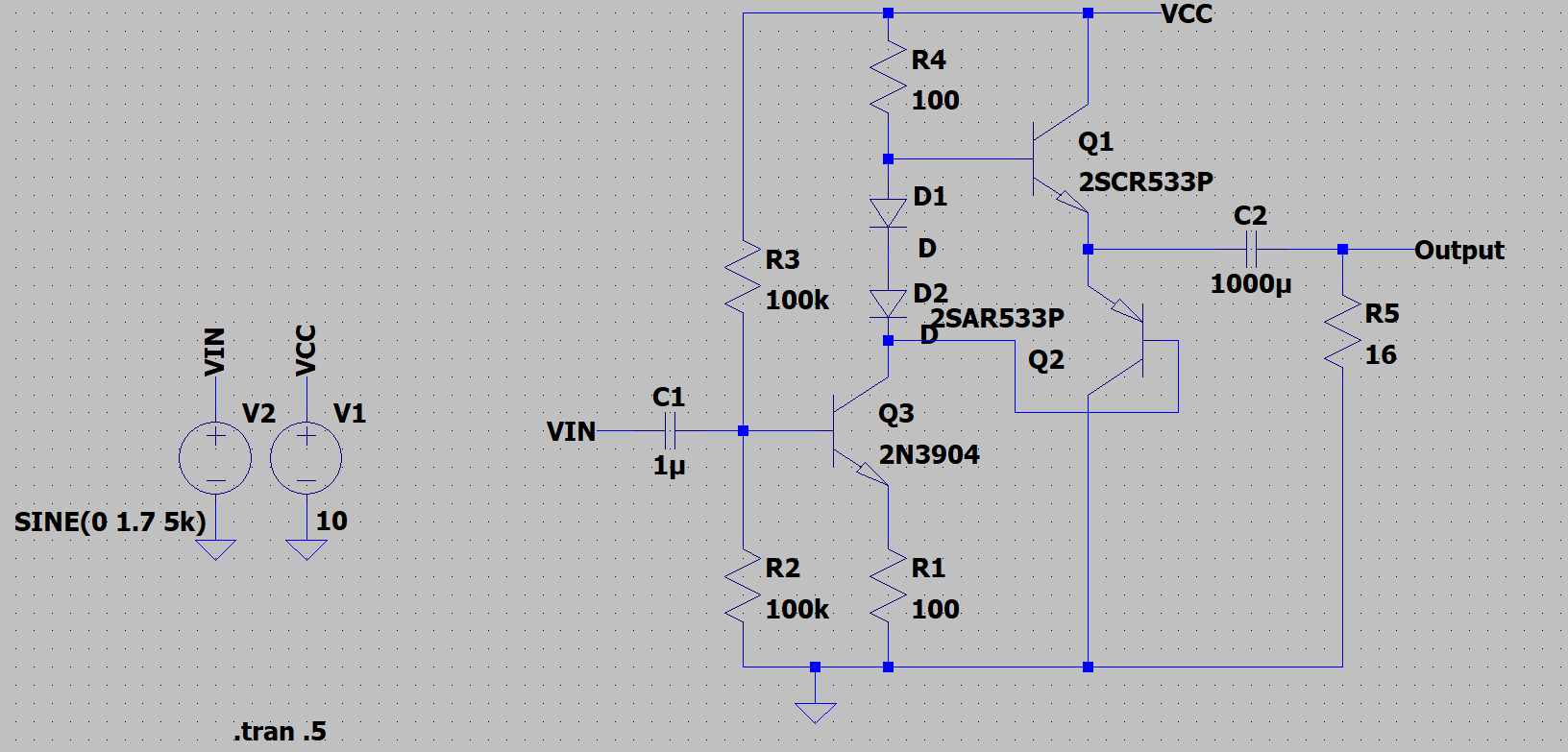
I have a 3 transistor Class AB power amplifier that I referenced from a working design which has different design parameters and biasing than what I need.

enter image description here

How I intend on using it, it will be used to drive a 16 ohm 2W speaker and the input is an AC signal with maximum 6V peak. Vcc needs to be 10V. I want 2W max output which requires 5.65V on the output, therefore I mainly want unity voltage gain and only current gain.

The issue is that I did some calculations and changed the voltage gain to 1 by adjusting R4/R1, and lowered the Q-point by adjusting R3 & R4 to allow for larger headroom to prevent output clipping when the input increases, but using calculations for finding Class A amp biasing values don't work because of the biasing diodes used for the push-pull output pair. And even by playing with the Q-point I still get clipping above 1.7V, and lowering the Q-point further starts to clip the bottom peak of the output.

enter image description here

In the simulation attached the green waveform is the input, blue is output of driver transistor's collector, red is the output for a 2V input sine wave.

What can I change to allow for the full input voltage to be seen unclipped at the output? Is it possible to set a Q-point that allows for full voltage swing that I need (11.3Vpp)? What calculations do I need or does this circuit only work with small amplitude input signals? Do I need a different circuit entirely?

For context this will be used as the final stage in a guitar amp project. Thanks in advance.

\$\endgroup\$
5
  • 4
    \$\begingroup\$ Q2 is upside-down. \$\endgroup\$
    – brhans
    Commented Nov 18, 2021 at 2:44
  • \$\begingroup\$ @brhans Thanks a lot for the reply. I thought the symbol in LTSpice was just weird but turns out by default it's upside down! That helps... I corrected it and now the output is changed. Now the gain can be set to 1 by setting R4/R1 = 1 as expected which is great. However I still have the output clipping when input goes beyond 1.7V. \$\endgroup\$
    – rustypwns
    Commented Nov 18, 2021 at 6:04
  • \$\begingroup\$ What values are you currently using for R1, R2, R3 and R4? \$\endgroup\$ Commented Nov 18, 2021 at 7:12
  • \$\begingroup\$ @BruceAbbott I'm currently using the values shown in the schematic posted. R4=R1=100 ohm and R2=R3=100k ohm \$\endgroup\$
    – rustypwns
    Commented Nov 18, 2021 at 7:23
  • \$\begingroup\$ What are the DC values in the circuit? It the blue waveform still holds for the driver collector stage output, then isn't it clear DC bias is too high and it clips? \$\endgroup\$
    – Justme
    Commented Nov 18, 2021 at 7:33

3 Answers 3

1
\$\begingroup\$

The configuration of Q3 with both collector and emitter resistors (R4 and R1) equal in value, does provide unity gain at this stage.

This also severely restricts the range of potentials you can achieve at the collector of Q3. Since both R4 and R1 pass roughly the same current, the voltage drop across them is always the same, and the lowest collector potential you can expect (without even considering diodes D1 and D2) is when both resistors have the greatest possible voltage across them. That is, half of the supply voltage \$V_{CC}\$. Q3's collector can't ever drop below \$\frac{V_{CC}}{2}\$.

The problem is worsened by biasing diodes D1 and D2, which "consume" 1.4V between them, so in practice Q3's collector is even further constrained, to between \$V_{CC}\$ and \$\frac{V_{CC}-1.4}{2}\$.

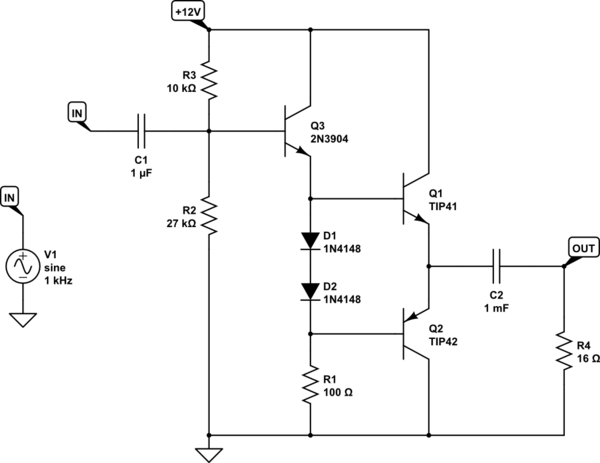
I believe your output is severely clipped, because Q3's collector is over-constrained. You may be better served by an emitter follower, with no such limitation, and unity gain:

schematic

simulate this circuit – Schematic created using CircuitLab

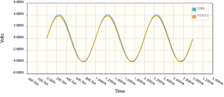
enter image description here

In this setup Q3's emitter can vary over almost the full power supply range, always being 0.7V lower in potential than its base.

Bias resistors R3 and R2 are an order of magnitude lower than the values you chose, because Q3's emitter resistor of 100Ω is quite a heavy load for Q3, and to bias it somewhere in the middle needs more base current than your original values would provide.

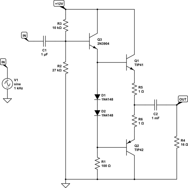
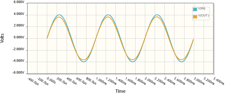
If you use the "simulate" link for the above schematic, you will find that the quiescent collector currents in Q1 and Q2 and very high, over 1A, which causes them to dissipate well over 6W even when there's no input. This is because biasing diodes tend to "over-bias" the transistors into quite heavy conduction. The usual way to mitigate this is to include ballast resistance between their emitters, to give those emitters some room to manoeuvre. The cost is slightly greater crossover distortion, and slightly reduced voltage gain:

schematic

simulate this circuit

enter image description here

\$\endgroup\$
1
  • \$\begingroup\$ You explained very well how Q3's collector voltage is being constricted, but why does the constricted collector voltage of Q3 cause the output to clip? I tried making modifications to my original circuit by reducing the magnitude of R3 and R2 to allow for greater base current into Q3 as well as other changes mentioned in the other answers and I got my output to push 3.1V without clipping. But your version with the emitter follower driver circuit has even better output range and power output so I'll be using this circuit. Thanks a lot for providing the circuit even with resistor and cap values! \$\endgroup\$
    – rustypwns
    Commented Nov 18, 2021 at 22:04
2
\$\begingroup\$

For 2W peak at the 16 Ohm load the output voltage has to be 2 x 5.65V = 11,3V peak to peak. In an ideal world you will lose in the emitters of the output transistors at least 0.7V meaning that you need to increase your supply voltage to 11.3 + 0.7 + 0.7 = 12.7V. But there is even more! Output transistors will lose gain as the signal approaches peaks and the current in the load increases, so they must be pushed harder from behind (driver transistor circuit biasing capability for the output transistors), and if it can not be possible, the real peak output voltage will be cut by at least another volt or more for each half cycle of the waveform. You need to add (roughly) 2V to the supply voltage, so it will have to be around 14.7V DC.

Now adjusting the gain: the schematic looks too much simple to be usable, but it will have as it is, a definite input impedance. Just add a resistor in series with your input capacitor so it can form a voltage divider, just try with values from 10k to 1Meg and there will be a value that lets you have correct ratio of voltage output vs voltage input.

\$\endgroup\$
1
  • \$\begingroup\$ Thanks for the input! I will settle for a smaller output voltage then since I need my supply voltage to be 10V. I took your advice as mentioned in other answers and added a series resistor to the input to reduce the gain. I'm using the new resistor R6 = 11k in series with C1, then changed the R4/R1 ratio to 1k/100, and also changed R3 to 12k and R2 to 1.5k. I can get up to 3.1V on the output now but I'm still hoping for a higher output with a 10V supply. Any more advice? \$\endgroup\$
    – rustypwns
    Commented Nov 18, 2021 at 20:45
1
\$\begingroup\$

The problem is that, for the dc biasing, you need a fairly large voltage across R4 and a smaller voltage across R1 in order to avoid both positive and negative clipping. To achieve, this R4 must have a larger value than R1 which of course will give the stage some gain.

So having achieved mid-supply(ish) biasing and fairly low Q3 emitter biasing by making R4 larger in value than R1 you then need to reduce the overall gain back down to unity by adding a large resistor in series with C1 which will form a potential divider with the input resistance of the stage.

So that the added resistor doesn't have to be too large you will need to reduce the values of R3 & R2 and adjust their ratio to get the required fairly low Q3 emitter biasing that's needed.

So basically, to get the required biasing, its a matter of increasing the gain by increasing the ratio of R4 to R1 and then reducing it back down by adding an extra resistor in series with C1.

You will need to play around to balance the base bias against the ratio of R4 to R1 against the size of the added input series resistor.

\$\endgroup\$
4
  • \$\begingroup\$ Thanks for this response, it was really helpful. Following your advice, I added a new resistor R6 = 11k in series with the input cap C1, then changed the R4/R1 ratio to 1k/100, and also changed R3 to 12k and R2 to 1.5k, and now I'm getting a much improved output. I'm now getting up to 4.5V input with a 3.1V output without clipping. Though I played around with the resistor values for hours and I can't seem to get it any better than this. Anything else I'm missing to get a larger output signal closer to 5V without clipping or is this as good as it gets? \$\endgroup\$
    – rustypwns
    Commented Nov 18, 2021 at 20:31
  • 1
    \$\begingroup\$ @rustypwns That's great, I expect that's been a really good learning exercise for you. You could try halving the values of both R4 and R1 to 500R and 50R respectively which will reduce the voltage drop across R4 due to Q1s base current. This change will increase the output bias, so reduce R3 a bit to, say 11k to bring the output bias back down a little. These changes will reduce the input resistance of the stage so you will then need to reduce R6 a little to get the benefit of the changes. Only a suggestion to try and see if there is an improvement in available output swing..... \$\endgroup\$
    – user173271
    Commented Nov 18, 2021 at 21:59
  • 1
    \$\begingroup\$ @rustypwns ..... only problem is, if you reduce the dc bias too much then the voltage at the emitter of Q3 could be too small compared with the Vbe of Q3 which would make the bias less stable with temperature. That is to say, too low a dc bias voltage at the emitter of Q3 and the dc bias of the output could shift as the output transistors warm up possibly causing clipping. \$\endgroup\$
    – user173271
    Commented Nov 18, 2021 at 22:04
  • \$\begingroup\$ The main reason I'm doing this project is to learn and review, and hopefully whatever information is shared here can help others too. It's actually hard to find resources and specific information on this without asking for help. These additional changes had a small effect compared to the large improvement from the initial changes you mentioned. I may end up using an emitter-follower driver stage suggested by the other answer instead of the current design. \$\endgroup\$
    – rustypwns
    Commented Nov 18, 2021 at 22:35

Your Answer

By clicking “Post Your Answer”, you agree to our terms of service and acknowledge you have read our privacy policy.

Not the answer you're looking for? Browse other questions tagged or ask your own question.