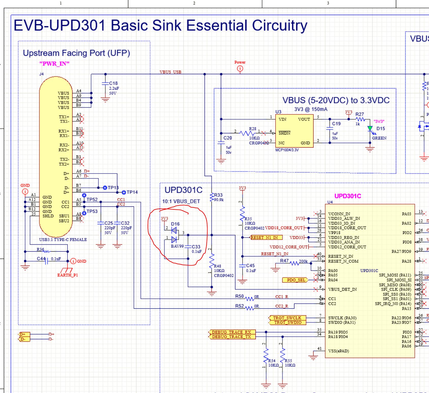
One could make the argument that it's unnecessary, yes.
It is a clamping diode, as mentioned by others. Note that BAV99 has a fairly high Vf, so that the MCU's input clamping (ESD) diodes are likely to be forward-biased as well -- they're basically in parallel, and so will share some undefined amount of current. We normally also prefer putting a series resistor (before the MCU pin) so that the current sharing is better defined: take Vf(max) at Ipk, subtract pin Vf (rarely documented; assume 0.6V), divide by pin Imax (e.g. 5mA), and this gives the resistance required to limit current safely.
This is ignoring particulars about what the chip is, what it's doing, etc.
If it's an MCU, likely the pin is an analog input, with Imax = 0 for normal operation; we need a better clamping strategy in that case. We could use schottky diodes (e.g. BAT54S), or a more complicated clamping arrangement.
Checking, I see UPD301C is a power management chip, and as evident from the pin name, it's likely special function, and may have a different ESD solution. Indeed, the datasheet says on p.30:
UPD301B/C Stand-alone USB Type-C Power Delivery 3.0 Controller
Maximum 4V (well, 3.96V; that's a very peculiar choice..). Note it is independent of supply voltage (contrast with the other pins being relative to VDD33_REG_IN), meaning they must have some kind of zener or snapback diode, not a clamp diode to VDD.
But we can go further. Also as mentioned by others, the only likely concern is ESD. (Cross-wiring would be the only other option, and pretty hard to do with USB connectors I would think!?) ESD is a very high voltage (8kV or even more), but it's a very brief pulse (~50ns) from a fairly modest source (1.5kohm, give or take which standard you're using). So, the peak current is quite high (>10A) during that pulse, but not a whole lot of charge is delivered.
So we can use the 3V3 supply for clamping, as long as it has adequate capacitance. C33, C19, and there are probably many others in the circuit as well, all act in parallel. A few uF is enough to get the peak voltage in a reasonable range.
But further: C18, C20 and maybe others already provide this service at the VBUS node itself. So any ESD seen by VBUS_DET_IN is likely very small indeed!
There is a final surge condition that can occur: when the input rises very sharply (and with little current limiting), the cable inductance can resonate with the input capacitance (C18, C20, etc.), doubling (or more!) the peak voltage.
Note this requires \$I_{in(pk)} \sim \frac{V_{bus}}{\sqrt{\frac{L}{C}}}\$, for L the cable inductance (ballpark 0.3uH/m), C the total bypass, and Vbus the nominal supply voltage (with the capacitors being initially discharged).
A simple solution is some lossy capacitance on VBUS (an electrolytic several times the total (ceramic) capacitance), or a TVS to clamp the peak voltage not much higher than nominal.
(The RLC series resonant circuit, has a step response of peak exactly twice the input. How could it be more? Ceramic capacitors: the capacitance drops as voltage rises. The C(V) curve is not flat as we would like, but substantially depressed. As the inductor charges to peak current, and VBUS charges past nominal, C drops precipitously, thus the inductance is effectively over-charged relative to the new value of capacitance -- voltage thus rises even faster, and shoots up to a peak easily 3x or higher. I recommend choosing ceramic caps only where you can see the C(V) characteristic curve, and selecting them to retain say 70% of nominal capacitance, at nominal voltage. Probably a 2.2uF would have to be 1206 sized or larger to meet this.)
Note that U3's limit is 30V as well, so this would be relevant under the necessary circumstances, and maybe other things off screen too.
Note, this probably should not happen with normal USB-C sources (with negotiated power, and limited peak current and slew rate).
On a completely different note, the grounding is insufficient. If EARTH_P1 must be kept separate, I would insist on at least four bypass caps in parallel, positioned around the connector, as close as possible to the pins/pads. If not separate, just hard-ground it to the internal ground plane.
ESD is most likely of all to strike the shield, dropping a huge voltage across this poor capacitor (100s of V -- the cap, traces and pins will total maybe 5nH, and the risetime is merely a few ns!), and thus disturbing the CCx and D+/- pins by as much (and RX/TX lanes, if they were in use). (This probably won't phase the, whatever's connected to the pins respectively -- this will be not much worse impedance than regular ESD, but at a much lower voltage, so much less energy/charge. It could still cause malfunction (corrupted data) or require a power cycle.)
This is also an RFI immunity concern.
(I'm not clear on if this is a design or review question, so take this as directed at readers interested in more of the design aspects.)

