0
\$\begingroup\$

I am currently programming an nRF24L01 using an ATmega328p microcontroller.

I have come across pin data direction. I have always used DDR in the past; for example, the first line below (DDRB) is familiar to me, but I do not understand DDB3, DDB4, and DDB5.

#define DDR_SPI     DDRB
#define DD_MOSI     DDB3
#define DD_MISO     DDB4
#define DD_SCK      DDB5

Any help would be appreciated.

\$\endgroup\$
1
  • 1
    \$\begingroup\$ DDRB means the whole register, DDB0 means Bit 0 of register DDRB \$\endgroup\$
    – Mike
    Commented Feb 27, 2023 at 6:59

2 Answers 2

2
\$\begingroup\$

DDB5 is to DDRB what PORTB5 is to PORTB; you can write DDRB |= (1<<DDB5) to set pin 5 of port B to output just like you can write PORTB |= (1<<PORTB5) to set pin 5 of port B high.

As far as I can tell, the values of DDB5 and PORTB5 are just 5 for every AVR chip there is, so the only reason to use them is if you think they have mnemonic value, or maybe to generate a compile error if your target doesn't have a PORTB (or doesn't have a pin 5 on that port?)

\$\endgroup\$
1
  • \$\begingroup\$ PORTB |= (1<<PORTB5) is to set pin high and DDRB |=(1<<PORTB5) to set the data direction so dont know why DDB5 have been used whats the advantage \$\endgroup\$
    – Yusuf
    Commented Feb 27, 2023 at 0:08
1
\$\begingroup\$

The mystery is revealed if we Read The Friendly Manual (Atmega328P datasheet): enter image description here
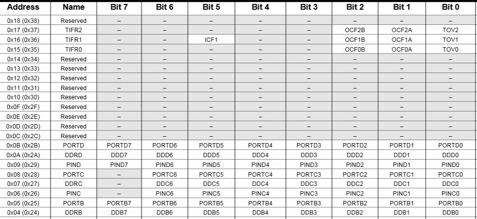
Here we can see that the bit masks are officially named DDB7 and so on from Atmel. (Arguably it would make more sense to name them DDRB7 but they didn't do that.) Always use the same bit mask names as stated in the manual. As we can see both DDB7 and PORTB7 will always be 0x80.

The reason why we use bit names is to avoid magic numbers. DDRB |= 0x80u; is less readable, as is DDRB |= (1u << 7);.

DDRB |= (1u << PORTB7); would just be confusing.

Although in practice you probably wouldn't be using these bit mask names directly, but those #defined for the hardware peripheral. In production code we might write:

DDR_SPI = (1u << DD_MOSI) | 
          (0u << DD_MISO) | 
          (1u << DD_SCK)  ;

Where (0u << DD_MISO) is 0 and is therefore only there as self-documenting code, stating that you intend for MISO to be an input.


As for what "DDR" stands for, on "Motorola-flavoured" MCUs like AVR, it means Data Direction Register. Motorola always named GPIO port registers as PORTX/DDRX and AVR picked it up from there.

\$\endgroup\$

Your Answer

By clicking “Post Your Answer”, you agree to our terms of service and acknowledge you have read our privacy policy.

Not the answer you're looking for? Browse other questions tagged or ask your own question.