2
\$\begingroup\$

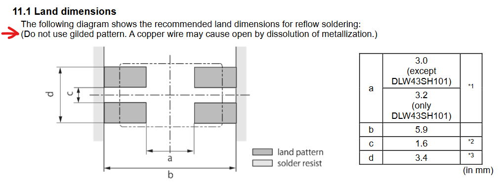
Looking at the recommended footprint for a CM choke, Murata# DLW43SH110XK2

aaa

It warns "Do not use gilded pattern". I've never noticed such a thing before

  • Should that be interpreted to mean no ENIG finish on the pads?
  • What does the cryptic note about dissolution mean here, and how likely is it?
  • Any impact on alternative finishes?
\$\endgroup\$
2
  • 1
    \$\begingroup\$ Gilded often means plated, or gold plated. Is your PCB going to be gold plated? Gold plating often needs special treatments or under-plating to hold up well on a copper surface layer. \$\endgroup\$
    – Nedd
    Commented Feb 21 at 1:25
  • \$\begingroup\$ @Nedd - finish on the pads, where they are not masked. ENIG (electroless nickel immersion gold) now common. I would have used it unless a reason not to \$\endgroup\$
    – Pete W
    Commented Feb 21 at 1:44

1 Answer 1

1
\$\begingroup\$

From the drawing on the component's datasheet it seems the bottom pads have the coil wires coming out to the four solder pad corners, likely copper wire. The note mentions that "A copper wire may cause dissolution of the metallization." This may indicate that the component's pads (with the copper wires) are not compatible with a plated (gold?) PCB pattern surface. Dissolution may just be an odd word for an adverse chemical reaction, or some other unfavorable metal to metal adhesion condition. If you use this component you may want to have the vendor mask off the component pads so they are not gold/ENIG plated.

\$\endgroup\$

Your Answer

By clicking “Post Your Answer”, you agree to our terms of service and acknowledge you have read our privacy policy.

Not the answer you're looking for? Browse other questions tagged or ask your own question.