1
\$\begingroup\$

I have a specific application in mind, but a more general question regarding diode stacks.

System overview:
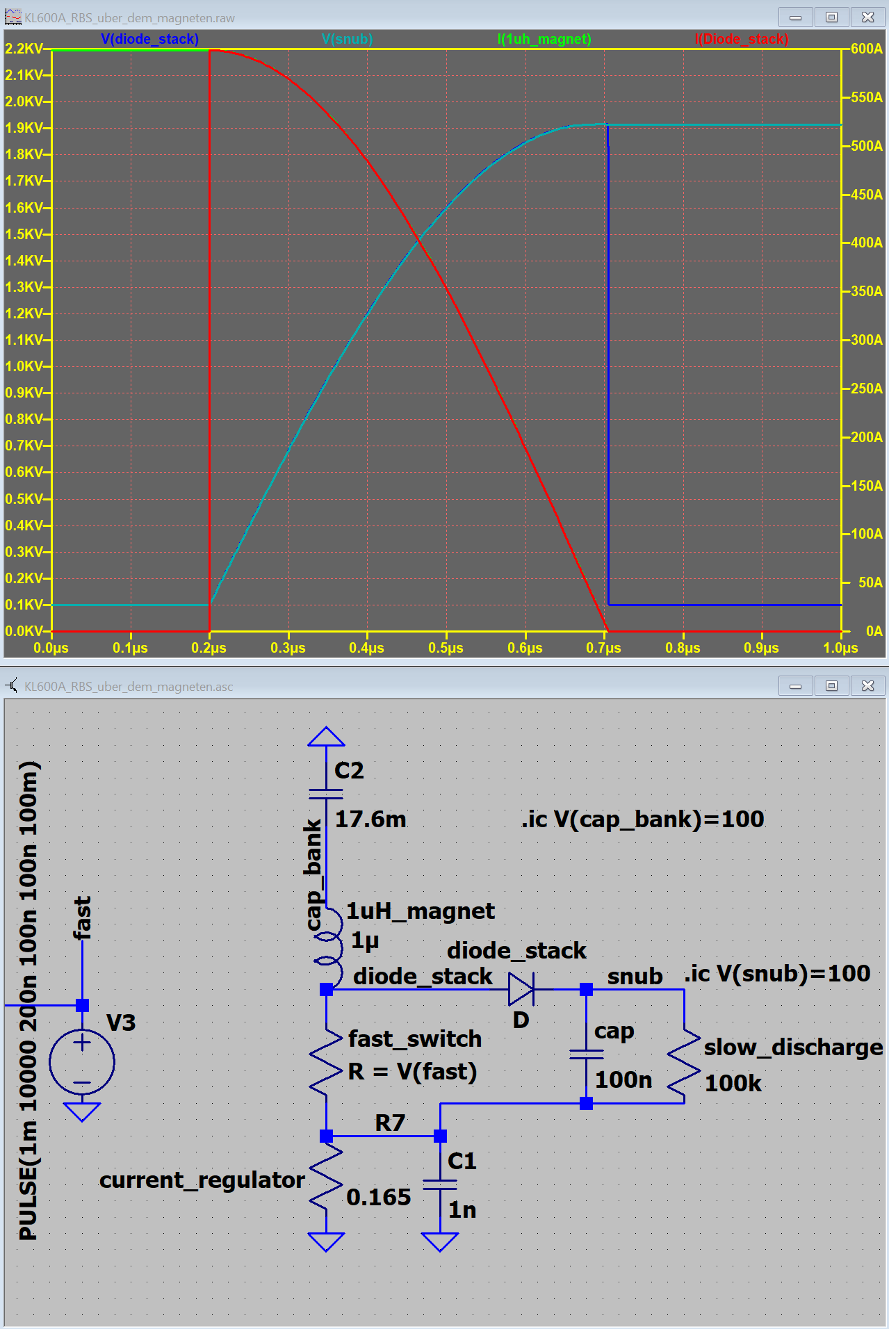
We have a constant-current source which is driving a constant current through a magnet. We need the current to stop fast (<1 μs) and without remaining current (<1%).

We have two different switches in the application. One is regulating the current "current_regulator" and the other one is stopping the current close to the magnet "fast_switch".
When the fast switch opens, the 600 A go through the diode into a 100 nF capacitor. The 100 kΩ resistor discharges the capacitor slowly. There is 100 ms before the next pulse.

Specific question regarding the diode stack:
We have "High Voltage Diode Assemblies" in our lab that can handle these currents and voltages easily, but they are costly.

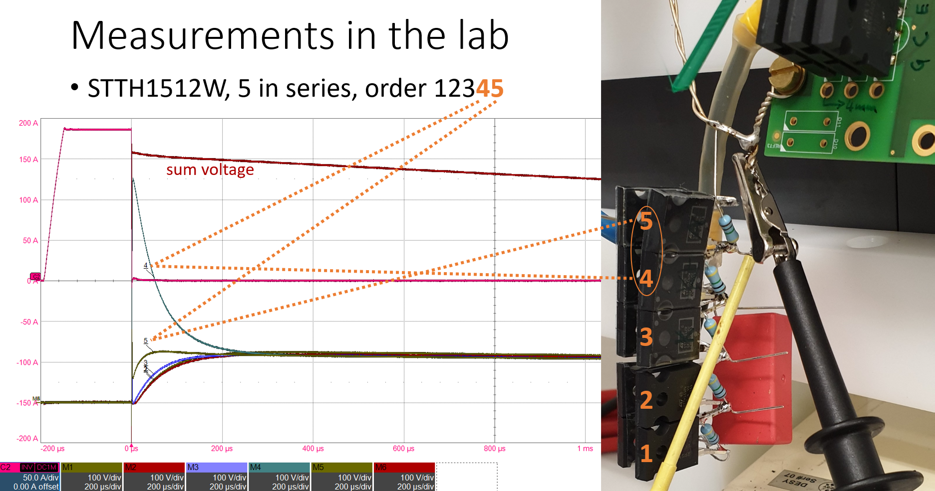
I know that I have to balance a diode stack with resistors and this works on a longer time scale. But during the initial switching moment (200 μs) the voltage across the diodes is distributed very unevenly. This means that when the current through the diodes stops flowing the reverse voltage is building up. Then for over 200 μs the voltage is balancing through the resistors.

I wanted to see whether the diodes or the mechanical setup were the problem and swapped the diode order from 12345 to 3 4 5 1 2, but the problem is always with the same diode and is not influenced by the diode position.

I went on and removed diodes 4 and 5 completely from the circuit, but then I had the same problem with diode 3. It looks like the diodes have different capacitances or stop conducting at slightly different times.

To measure the voltages I used a "TT - SI 9010A differential probe", input impedance is 50 MΩ and 10 pF. I also tried to add the five curves in the scope and compare the result with the measured voltage over all 5 diodes in series. The curves look identical.

I used STTH1512W diodes that I bought in the same package from a distributor; the date codes are also identical.

Now I have hopefully given enough information and still not so much that nobody is willing to read this. But I would be very curious what I have to do to get a balanced and fast diode stack, preferably even faster than 100 ns.

The diode would probably not be my first choice, but I had it available. Are there maybe diodes that should be used instead? Although I have a rather high current of up to 600 A, the current only flows for about 1 μs and only ten times per second.
I would like to stack many more diodes in the future but before I can do that I have to understand the underlying problems.

Thanks for you time.

diode stack with 1Mohm resistors

simulation of the whole circuit

\$\endgroup\$

1 Answer 1

0
\$\begingroup\$

Yes, in general, diode recovery doesn't match, even from parts of a given production run (maybe even wafer). Diodes are diffused devices, and diffusion is a notoriously tricky and precise operation; it is very challenging to get consistent doping profiles even across a wafer, let alone between wafers.

Stacks need to be built from selected (sorted, matched) parts to ensure equal recovery. Moreover, temperatures need to be matched -- stacks are typically packaged together, or even made of bare dies metallurgically bonded together so their temperatures track well. Thermal matching might not be a problem here in a pulsed application, but it is worth mentioning for completeness.

To match parts, you could set up a double-pulse tester with a MOSFET/IGBT, diode and inductor, and apply consistent conditions to each one. Measure the resulting recovery transient, and sort parts by trr and Irr.

An old trick you may be able to employ here, is paralleling them with capacitors, to swamp out individual differences in capacitance. These will need to be on the order of CJO (≫50pF), and will reduce performance of the system; a necessary compromise. Recovery can also be swamped, but this will take much more capacitance, probably more than you can afford here.

Capacitance can of course be measured in the usual way; a DMM capacitance mode will likely suffice, for example, perhaps including a large coupling capacitor (1µF+?) to avoid rectification. Make sure the bias voltage is consistent between tests, as CJO varies with bias voltage.


Unrelated, but worth mentioning: beware of the peak current rating. The short-pulse rating is often not much more than the mains inrush rating (and indeed both data are provided for this part, and are equal), and spooky failures can occur from exceeding this rating -- the device might not actually heat up at all, yet it fails shorted. Possibly the mechanism is electromigration, spot heating, or something like that, but in any case, the rating must be respected.

My anecdote on this: early in my career, while testing a high frequency (for the time) inverter board, having applied all the usual (read: wrong) rules of thumb, I had created an output with fully 80% voltage overshoot. On a 650V-supplied inverter, this was problematic. Well first of all, this necessitated 1200V MOSFETs, which were particularly inferior (early 2010s, SJ types hadn't filtered up to these product lines yet, so these were planar types, suffering from the classical quadratic RDS(on) vs. VDS(max) handicap), but on top of that, I needed to find ways to deal with this before ordering a revision.

I tried clamping the pulses directly, adding opposing-body-diodes (as it were) as close on the PCB as possible, so that when an opposing transistor turns on, the present transistor's voltage overshoot gets clamped to the local supply rail (four-layer board, inductance to the supply bypass caps was pleasantly low). This delivered pulses of about 80A and 50ns to the poor diodes, which experienced an impressive 60V apparent forward recovery voltage (only maybe 1/3 of which I could attribute to lead inductance), and despite the low average current (this was a at a few hundred kHz), even 12A rectifiers would eventually fail -- in some seconds to minutes. Finally, I chose 1200V 30A parts, and the prototype operated reliably -- if at poor efficiency for all the hackery.

After several revisions, and proving to myself, by recreating the scenario in SPICE, how fatally wrong "rules of thumb" can be; the eventual design worked smoothly, using a modest supply inductance to limit dI/dt, and an RCD clamp snubber. Typical numbers were something like, I think, 5kW total output power (VAs), 100W switching loss at up to 400kHz, varying with load phase: maximum for unloaded/capacitive output, maximum at full rated (somewhat to highly inductive) load, minimum switching loss (20W-ish?) at light inductive load (ZVS).)

Anyway -- 600A peak into -- it looks like you have two in parallel there? Two diodes, rated 200A each, is probably okay for a little while, but I would put a 3rd in just in case.

Mmmh... keep in mind, each of those paralleled parts needs to be matched too. This is gonna be a bit tedious, I'm afraid. (Those "expensive" stacks are starting to look attractive, no? 😅 )

Good luck, and keep those safety glasses handy! And probably hearing protection too, heh.

\$\endgroup\$
1
  • \$\begingroup\$ Thank you for your detailed answer. Since we do not produce large quantities of devices it actually looks like buying stacks might be the better option than spending a long to measure each individual diode. I would like to try it but it just isn´t worth if probably. If I actually find time to do it and get interesting results I will come back and add an answer to this post. And if somebody is interested in more details please let me know. \$\endgroup\$ Commented Apr 25 at 5:55

Your Answer

By clicking “Post Your Answer”, you agree to our terms of service and acknowledge you have read our privacy policy.

Not the answer you're looking for? Browse other questions tagged or ask your own question.