5
\$\begingroup\$

Okay so the foundation for my curiosity is that in dealing with Arduinos, I found they can be used to program the similar but smaller ATtiny chips. This is the main hookup configuration that some of you may be familiar with if you've done this before.
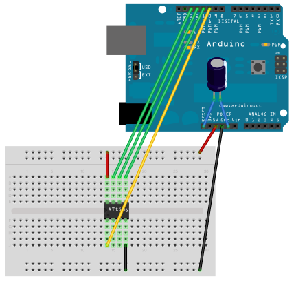
enter image description here

My problem then is I want to create a shield that sits atop the arduino and has multiple sockets for ATtinys, and a selector switch that allows for choosing which ATtiny is being programmed to.

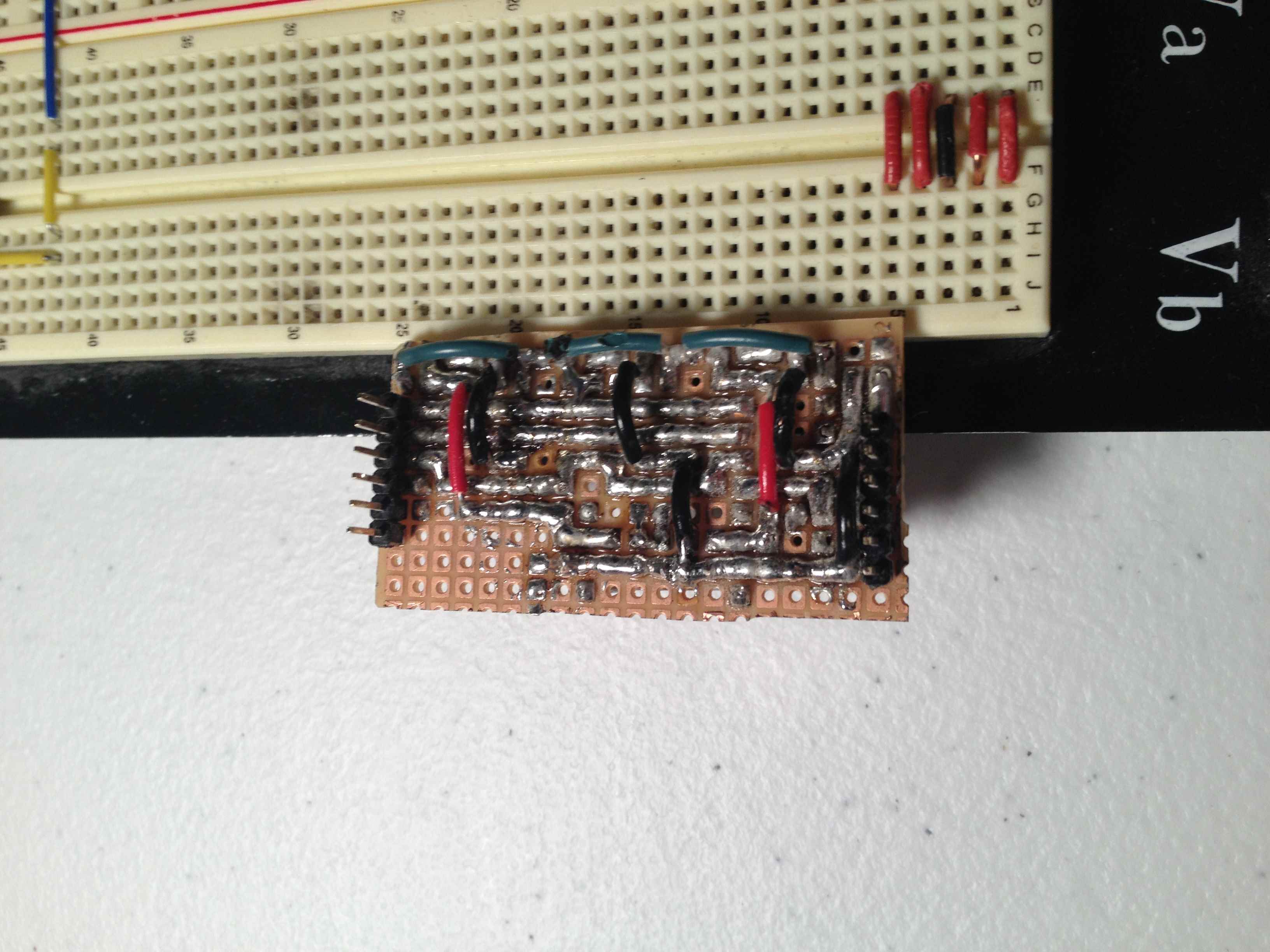
I actually did make a prototype, and here's what it looks like.
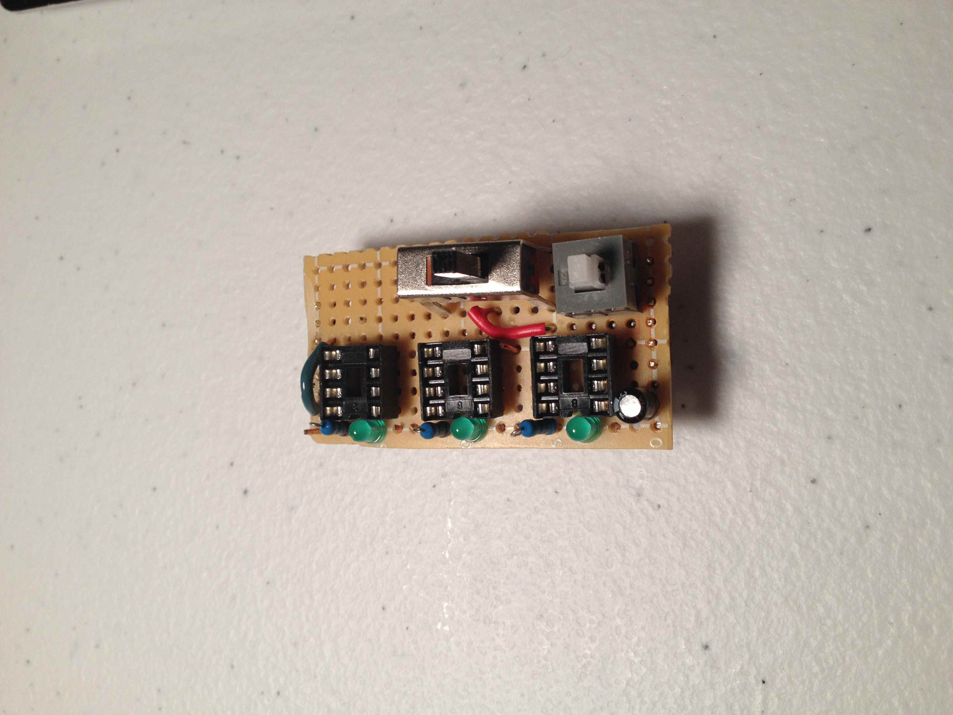
enter image description here

Not the easiest thing to solder!

enter image description here

So it just has a power switch and a simple single pole triple throw. Now I figured the best way to do it was to connect all of them to ground, and let the SPTT choose between which was powered. And in order to make the board as simple as possible, I connected the 4 data lines (3 green and 1 yellow in the picture) straight down and all 3 ATtiny's are connected in parallel to the data, regardless of if they are powered.

Of course this board fails though because I incorrectly assumed there would be no leakage through the ATtiny's data lines, and there is, so the other 2 that aren't being programmed weakly connect through the micro to their respective grounds.

Here's a schematic of it, just pretend it's a SPTT instead of SPDT.

enter image description here

Okay to the point. Effectively what I want is a device that performs this function. Would this be considered a mux?
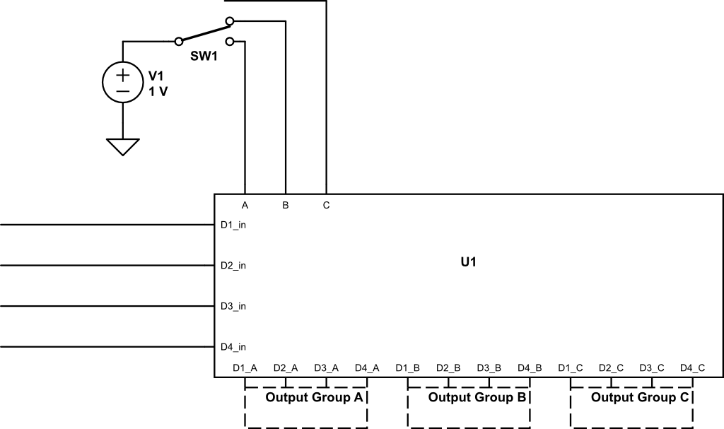
enter image description here

\$\endgroup\$
21
  • 1
    \$\begingroup\$ Not an answer to the actual question, therefore only a comment. It is probably enough to switch the \$\overline{\text{RESET}}\$ pin. The programming protocol defines strict timing with regard to this signal and thus if that signal is not present then nothing happens. Best to tie unused controller's \$\overline{\text{RESET}}\$ to ground so you can be sure all outputs will be in high impedance mode. Then you route the programmer's \$\overline{\text{RESET}}\$ pin to the device you actually want to program. \$\endgroup\$
    – jippie
    Commented Sep 8, 2013 at 20:03
  • \$\begingroup\$ 1. you tie all unused controller's \$\overline{\text{RESET}}\$ to ground (use a resistor so it can be overriden by your switch), resulting in all pins going into high impedance mode. 2. tie the \$\overline{\text{RESET}}\$ of the controller you want to program to the programmer's pin10 (in this case). \$\endgroup\$
    – jippie
    Commented Sep 8, 2013 at 20:09
  • \$\begingroup\$ So in other words: 1) Put pulldowns on each ATtiny's reset pins to GND, and switch the yellow line from the programmer to each ATtiny? Does this mean I don't need to switch the supply? \$\endgroup\$
    – krb686
    Commented Sep 8, 2013 at 20:10
  • \$\begingroup\$ I didn't try it, but I think that should work just fine. It's worth to try, you can't get a much simpler circuit. \$\endgroup\$
    – jippie
    Commented Sep 8, 2013 at 20:11
  • 2
    \$\begingroup\$ Sorry, you want me to put microscopic photos next time? That's so you can see it in detail cause lots of people complain about photos being too small. And yes the arduino image does provide useful information, it shows how the arduino is connected to the ATtiny, and it's there to give background about what I'm trying to do. Anyone else who has also done this would recognize that image from the very popular tutorial at HLTMedia I believe most people use. Just can't please em all I suppose \$\endgroup\$
    – krb686
    Commented Sep 8, 2013 at 20:52

2 Answers 2

2
\$\begingroup\$

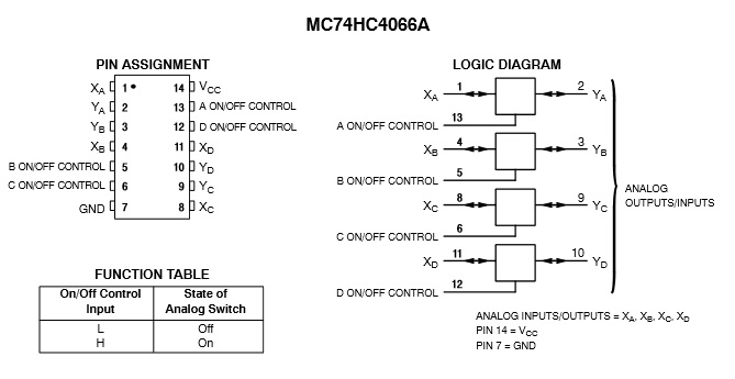
I recommend that you use three 4066 analog switches, with the 4 inputs of each chip wired in common with the inputs of the other chips, and the four control lines of each chip tied together and connected to your rotary switch.

enter image description here

Although this requires three chips, they are in a 14-pin DIP package so they are easy to wire up, and each can be selected by a single input (no decode), lending itself to the rotary switch in your diagram.

I have used these same devices (in a SMD package) to switch the four active leads (VCC detect, PGEC, PGED and MCLR) of a PIC programmer, and it works just fine.

The chip has a typical Ron (resistance between the inputs and outputs) of 80 Ω, but that does not seem to affect the operation of the programmer. There are some quad bilateral switches available with a lower Ron, but they are only available in SMT packages.

\$\endgroup\$
11
  • \$\begingroup\$ Very nice! This looks what I need. Would this be different from using tri-state buffers, though? I'm guessing tri-state buffers are a one-way only so I'd need to hook some of them up backwards for the communication from ATtiny to programmer. Other than that, any difference? I'm sure this would be better if communications needed to be 2-way but I don't think it's necessary in this case. \$\endgroup\$
    – krb686
    Commented Sep 8, 2013 at 22:25
  • \$\begingroup\$ I'm not familiar with the programming signals for the ATtiny chips, but I know for the PIC at least one of the signals (PGED, or data) is bidirectional since the programmer needs to both write and read from the chip. So you are better off using a chip like the 4066. \$\endgroup\$
    – tcrosley
    Commented Sep 8, 2013 at 22:37
  • \$\begingroup\$ Sounds like a good idea. Now if only they made an IC that had multiples of the 4066's with control bits internally tied, so I could get away with a single IC with ~24 ish pins! \$\endgroup\$
    – krb686
    Commented Sep 8, 2013 at 22:44
  • \$\begingroup\$ Hey whaddya know, it looks like they just might! Here's an IC that is essentially 2 4066's combined, in a 16-pin DIP package mouser.com/ds/2/308/MC14551B-D-96744.pdf \$\endgroup\$
    – krb686
    Commented Sep 8, 2013 at 22:48
  • \$\begingroup\$ @krb686 The problem with this approach is you can't turn both the outputs off; one output is active with an input of 0, and the other one with an input of 1. \$\endgroup\$
    – tcrosley
    Commented Sep 8, 2013 at 23:04
2
\$\begingroup\$

What you want is a analog bus switch or multiplexer. Analog meaning it's not digitally controlled (serial/i2c/spi). A 4 bit (or quad) 3 to 1 (or higher, 4 to 1, 5 to 1, 5 to 2, etc) switch would be best, as it would be an all in one solution for your 4 wire, 3 IC setup.

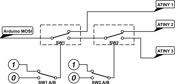
An ever so slightly more complex, if not cheaper and easier solution to implement because they are easier to find, would be to use two 2:1 multiplexers/switches. The Switched side of one will lead to either an Attiny, or to the second bus switch, which leads to the other two Attinys. Below is a representative schematic. Any 4 bit 2:1 multiplexer will do.

schematic

simulate this circuit – Schematic created using CircuitLab

\$\endgroup\$
3
  • \$\begingroup\$ Still can't seem to find a component that satisfies this requirement. I've searched for bus switches and multiplexers, and the best I've found matches what I linked in the comments on tcrosley's answer, an IC that can switch 4 lines to 2 separate groups of 4 outputs. I've yet to see any component that can switch to more than 2 output groups. \$\endgroup\$
    – krb686
    Commented Sep 9, 2013 at 14:42
  • \$\begingroup\$ Well I did just find this. It switches 4 sets of 4 data line inputs all to a single 4-set output. What I want is the exact opposite. I guess I need a quad 1:4 mux engineering.uiowa.edu/sites/default/files/ees/files/NI/pdfs/01/… \$\endgroup\$
    – krb686
    Commented Sep 9, 2013 at 14:51
  • \$\begingroup\$ @krb686 remember, the miso line is the reverse direction of the other three lines. And I think you are too hung up on wanting a single chip. 4:1 bus switches are often set up as three cascading 2:1 bus switches. \$\endgroup\$
    – Passerby
    Commented Sep 10, 2013 at 8:28

Your Answer

By clicking “Post Your Answer”, you agree to our terms of service and acknowledge you have read our privacy policy.

Not the answer you're looking for? Browse other questions tagged or ask your own question.