1
\$\begingroup\$

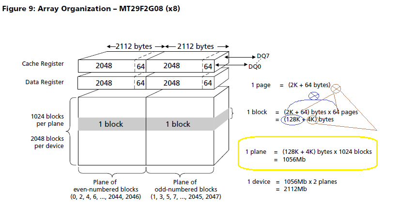
Could you please explain how memory array organization calculated? Here I have attached snapshot of 2Gb NAND flash memory array organization. I can't understand the calculation of 1 Plane (marked in yellow color), but I do understand the calculation of 1 block.

enter image description here

\$\endgroup\$
1
  • \$\begingroup\$ thank you very much for your correction of my sentence formation. \$\endgroup\$
    – Ram_HW
    Commented Jul 1, 2015 at 11:32

2 Answers 2

1
\$\begingroup\$

The image of the part number you have shared implies that its a 2-Plane NAND Flash chip.

A Page is 2,048 + 64 Bytes long, 64 such pages forms one Block.

So,

size of 1 Block = size of 64 Pages
                = 2,112 x 64 Bytes
                = 1,35,168 Bytes
                = 10,81,344 bits
                = 1056 Kb

Now, 1 Plane consists of 1024 such Blocks. So,

size of 1 Plane = 1024 x 2112 x 64 Bytes 
                = 1024 x 1056 Kb
                = 13,84,12,032 Bytes
                = 1,10,72,96,256 bits
                = 1,056 Mb

Since the device has two such planes, Memory size of 1 Device = 1,056 x 2 = 2,112 Mb.

Kindly note that 2112 Bytes each for Cache Register and Data Register are not being counted in the sum of total memory, since it is not a non-volatile memory.

Additionally, the advantage of having two blocks is:

  • Memory can be divided into two physical planes, odd/even blocks
  • Users have the ability to:
    <•> Concurrently access two pages for read
    <•> Erase two blocks concurrently
    <•> Program two pages concurrently
    Provided that, the page addresses of blocks from both planes must be the same during two-plane Read/Program/Erase operations.
\$\endgroup\$
1
  • \$\begingroup\$ ya i got it clearly thanks . But my mistake i was not watched carefully the calculation of plane as byte to bit conversion. \$\endgroup\$
    – Ram_HW
    Commented Jul 2, 2015 at 5:13
1
\$\begingroup\$

This NAND Flash Memory is an example of 64bit system based modern flash memeory both fast and huge,the thing with the modern cards the company uses a standard system for making various sized/capacity chips, here the technology PML 5(Page Map level 5) is used for extended address handling,

A page is a virtual memory block in device hand hence the basic page size according to your Fig. is.

=(2048 +64) or (2K + 64)    where 2K=2^10

=64 x 8 bit = 64 bytes(these value really depend upon the page table structure (PML5*)        

=2048*8 bit=2K* 8 bit=2K byte

PML is a type for the page tables structures.For more info on IA-32 structure see Physical Adress Extension.

Now lets see some details as you can see that a page has a total size of   2K+64 bytes Now you see that we are using Segmented Memory, A segmented memory has two banks ,one bank is even bank and the other is called the odd bank containing all the odd addressable byte.You can read more about Memory Segmentation.

A whole block has 64 pages, these may vary per design,but they are standard for 64 bit systems. To sum overall discussion
Device has 2,048 blocks organized as 64 ....a total of 2,112-byte (2,048 + 64 bytes) pages per block. Each block is 132K bytes (128K + 4K bytes).Each plane has 1024 blocks per plane and 2 planes per card thats your device.

So why use this system,often Companies use these blocks,they use standard memory addressing page structure for all the cards hence while moving up the total capacity(2GB to 64 GB) all they have to do is just add one stack of die over the other,as the system design remains the same,hence its adds modularity in die designing.

* I really doubt the Technology used its just for refrence of the OP I have specified a category

\$\endgroup\$
0

Your Answer

By clicking “Post Your Answer”, you agree to our terms of service and acknowledge you have read our privacy policy.

Not the answer you're looking for? Browse other questions tagged or ask your own question.