4
\$\begingroup\$

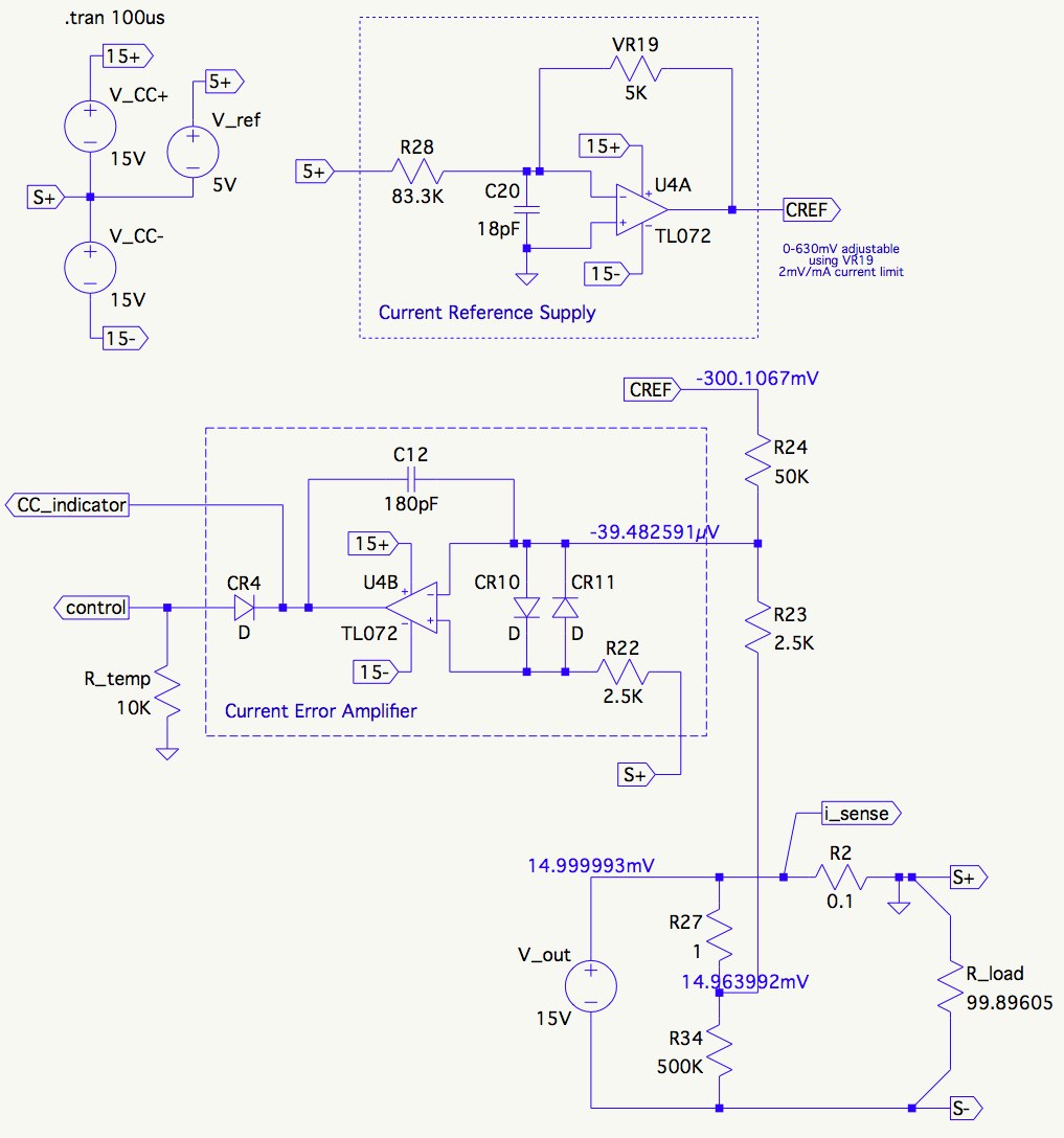
I'm studying the constant-current circuit of the Agilent E3610A 15V 30W DC Bench Power Supply. The entire schematic is at the end of the user manual, but I've redrawn the parts of interest here for clarity.

enter image description here

The current reference supply provides a reference voltage of 2mV/mA of current limit. Its level is adjustable via VR19, a 10-turn pot on the front panel. This part of the schematic is simplified to reduce max output and I'm showing a TL072 instead of the original LF411, but it's a pretty straightforward inverting amplifier.

The current error amplifier is also a straightforward inverting amp driving the control node. It takes its input error signal from a resistive summing point formed by R23 and R24. When the current is being limited, the value of the summing point is close to 0V. Note that S+ is ground, even though it's the positive output of the supply. The overall DC supply is an inverting amp, so somewhat counter-intuitively, the output voltage is S-.

My question is about the circuit around the current sample node labeled i_sense. A voltage of 100mV/A is developed across R2, which acts as the current sampling resistor.

Unexpectedly, to me at least, the current sample voltage is connected via a lopsided resistive divider (500k/500.001k) formed by R27 and R34.

What's up with that? Why isn't R23 connected directly to the i_sense node?

After studying it for some time, all I have is some vague guesses:

  • It has something to do with behavior when the output is shorted ...
  • It somehow shunts the sampling current around the current sampling resistor itself to increase accuracy

.. neither of which I'm able to make work in my head.

Can anyone help me understand? I'm pretty sure it's this way for a good reason :)

\$\endgroup\$

2 Answers 2

2
\$\begingroup\$

The divider of R34 and R27 appears to allow the current limit point to be a function of \$V_{\text{out}}\$. At low \$V_{\text{out}}\$ U4B will perceive closer to the full \$I_o\$. As \$V_{\text{out}}\$ increases, perceived \$I_o\$ will be reduced, allowing more \$I_o\$.

I haven't looked at any numbers to see how large an effect this would be. It could be part of a foldback current limit, although, just looking, it doesn't seem like it would be enough for that. It could also be a way to sharpen the slope of \$V_{\text{out}}\$ reduction during current limit. Maybe gain of the current loop isn't quite enough to keep \$I_o\$ constant during limit.


A Closer Look at \$I_{\text{o-set}}\$

Looking at the Current Error Amplifier, and Voltage Output sections of the schematic, an equation for U4B-inv as a function of Cref, \$I_o\$, and \$V_{\text{out}}\$ can be written.

\$V_{\text{U4B-inv}}\$ = \$\frac{\text{Cref } (\text{R2} (\text{R27}+\text{R34})+\text{R23} (\text{R27}+\text{R34})+\text{R27} \text{R34})+\text{R24} \left(-\text{R27} V_{\text{out}}+I_o \text{R2} (\text{R27}+\text{R34})\right)}{\text{R2} (\text{R27}+\text{R34})+\text{R23} (\text{R27}+\text{R34})+\text{R24} \text{R27}+\text{R24} \text{R34}+\text{R27} \text{R34}}\$

When the current loop becomes active, during constant current regulation, and for a perfect OpAmp, \$V_{\text{U4B-inv}}\$ = 0V. The equation can be turned around and written for the current limit set point (\$I_{\text{o-set}}\$) as a function of Cref and \$V_{\text{out}}\$.

\$I_{\text{o-set}}\$ = \$\frac{\text{R24 } \text{R27 } V_{\text{out}}-\text{Cref } (\text{R2} (\text{R27}+\text{R34})+\text{R23} (\text{R27}+\text{R34})+\text{R27 } \text{R34})}{\text{R2 } \text{R24} (\text{R27}+\text{R34})}\$

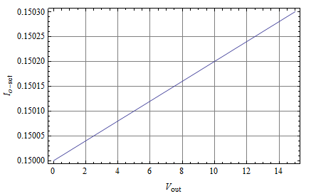
\$I_{\text{o-set}}\$ relationship to \$V_{\text{out}}\$ is set by R2=0.1 Ohm, R24=50kOhm, R27=1 Ohm, R34=500kOhm. \$I_{\text{o-set}}\$ will be adjusted by \$V_{\text{out}}\$ at a rate of \$20\mu A/V\$. Here's a chart to better show what this looks like:

enter image description here

Value for Cref was -.29987, because it gave nice even numbers. For a 15V change of \$V_{\text{out}}\$ results in a \$300\mu A\$ change of \$I_{\text{o-set}}\$. It may not seem like much, but it is in the right ballpark to correct gain error in the current loop to maintain a constant current load regulation.

It looks like your second guess was closest to right: Divider R27, R34 is most likely used to improve constant current regulation.

One way to check would be to short R27 and operate in constant current mode. Then you could see the error of regulation without any correction.

\$\endgroup\$
8
  • \$\begingroup\$ I ran some figures on it, and you're right, the voltage at R34/R27 (let's call it \$V_S\$) is reduced by increasing \$V_{out}\$, but the difference comes to some tens of nV (nano·Volts). This is indeed a conundrum :) \$\endgroup\$
    – scanny
    Commented Oct 25, 2015 at 3:55
  • \$\begingroup\$ @scanny, I would have expected it to be something more like \$V_{\text{out}}\$/500K. It's a bit late for conundrums tonight. ;^) \$\endgroup\$
    – user16497
    Commented Oct 25, 2015 at 4:27
  • \$\begingroup\$ Oops, Excel formula scaling factor error there, should be some tens of microvolts! I was thinking nanovolts seemed a bit wack :) Still though, pretty small, don't you think? The front panel resolution for current is 10mA, so I'm not seeing how the voltage difference could affect the current limit level in a noticeable way. \$\endgroup\$
    – scanny
    Commented Oct 25, 2015 at 4:39
  • \$\begingroup\$ Ok, I have a new hypothesis. I just noticed that on the bench, I can't get the current limit below about 5mA. I think this may be largely because my pot doesn't go all the way to 0Ω, but it got me thinking. Could this be there to guarantee you can set the limit all the way down to zero even against some offset current or something? \$\endgroup\$
    – scanny
    Commented Oct 25, 2015 at 6:57
  • \$\begingroup\$ @scanny, I don't think it's there to manage an offset. It doesn't seem to go the right way for that. Also I don't think you would want to do that as a function of \$V_{\text{out}}\$. \$\endgroup\$
    – user16497
    Commented Oct 25, 2015 at 22:40
2
\$\begingroup\$

Heavily weighted dividers like that generally find use when a given input must not achieve Vcc. Many instrumentation amplifiers have an input maximum voltage that is specified as being no larger than a certain percentage of the power rails. Specifically, if the input goes to full Vcc in either polarity, there is usually a fair chance that the chip itself can't handle the potential difference between that and the opposing rail - this is especially true when the chip is being used with its maximum supply rail voltages.

Edit: However true that may be, I missed what was happening here. (Sorry, on a road trip.)

This divider inserts a guaranteed offset from 0. The control output is most likely built to recognize and respond to a loss of input with some kind of alarm or code in the event that i_sense becomes true zero, indicating a loss of signal. Without looking, I'd say that would result in the output simply being turned off, for reasons of safety.

\$\endgroup\$
3
  • \$\begingroup\$ The maximum potential of the i_sense node would be about 300mV in the original circuit, corresponding to a current of 3A. So I'm not seeing where we'd be approaching \$V_{CC}\$ (15V) or how the 1Ω resistor would change that at all. You saw that S+ is ground (0V), right? It's the reference for \$V_{CC}\$, and, well, everything else too :) Also, in this circuit the diodes CR10 and CR11 keep the inverting input voltage in the range -0.7 to 0.7V. \$\endgroup\$
    – scanny
    Commented Oct 24, 2015 at 23:34
  • \$\begingroup\$ @scanny - I see it now. And I bet I know why. Edit coming. \$\endgroup\$
    – user39962
    Commented Oct 24, 2015 at 23:43
  • \$\begingroup\$ Okay, this is interesting, that certainly is more plausible than any answer I'd dreamed up so far :) One thing puzzles me about this though. There would still be a magic output current for any given output voltage that would yield a zero sample voltage, because the potential of the R27/R34 junction will always be less than \$V_{isense}\$. The simple case would be (0V, 0A), but could also be (5V, 100µA) or something. I do notice the sampling draws about 6µA, which actually reduces the sample voltage by about 6µV. Also, I don't see how the logic board could see that voltage without a connection. \$\endgroup\$
    – scanny
    Commented Oct 25, 2015 at 0:48

Your Answer

By clicking “Post Your Answer”, you agree to our terms of service and acknowledge you have read our privacy policy.

Not the answer you're looking for? Browse other questions tagged or ask your own question.