0
\$\begingroup\$

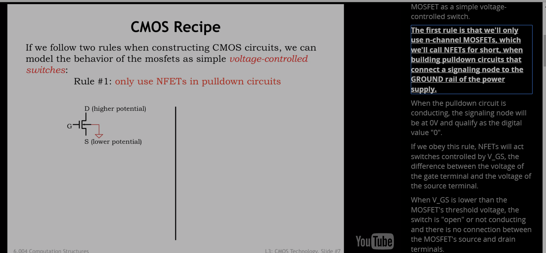
enter image description here

See pic

  1. EDIT: The original youtube video link: https://www.youtube.com/watch?v=3XpzgvUDVDQ

  2. What is a signaling node?

  3. Why do I have four nodes? I thought MOSFET's had 3 pins

  4. Why does connecting the signaling node to ground give us the switch behavior we want?

\$\endgroup\$
3
  • \$\begingroup\$ Please embed the image in the question rather than provide a link. \$\endgroup\$
    – Transistor
    Commented Dec 19, 2015 at 22:37
  • \$\begingroup\$ It's basically poppycock what they are saying, please try and do some better research on MOSFETs if you want to understand them. Don't use that document to do research on MOSFETs. Rule #1 is just garbage when you start looking at H bridges. \$\endgroup\$
    – Andy aka
    Commented Dec 20, 2015 at 0:41
  • \$\begingroup\$ @Andyaka, I can't tell for sure, because there is not enough context. But I think this is a tutorial on understanding CMOS logic. If the rule is meant to apply only to that specific case, then I think it is probably an OK rule. \$\endgroup\$
    – user57037
    Commented Dec 20, 2015 at 2:41

1 Answer 1

1
\$\begingroup\$

1) I watched the video.

2) In this case, the term "signalling node" refers to the drain of the NFET. In other words, the output you are trying to design

3) Do not worry about the 4th node until later. For now, ignore it. It is the body node in the MOSFET. Generally you are going to connect it to the source.

4) You are going to have to be a little more patient, watch more of the videos in this series. They are trying to present you with a set of simple rules for designing CMOS digital logic. What NMOS does is short drain to source when the gate voltage is higher than the source voltage. Whether this gives you the switching behavior you want depends on you. You have to design the circuit so that the output behaves the way you want based on the input.

Basically what they are saying in this video is that in CMOS logic, you put NFET on the bottom and PFET on the top. In both cases, the drain is the output (which they also seem to be calling the "signalling node.") The source is grounded for NMOS and connected to VDD for PMOS. A high on the gate will cause the output to be low (for an inverter). Because high turns ON NMOS and turns OFF PMOS.

The fourth terminal is available to IC designers only. That is why you have not encountered it. On discrete MOSFET's, the body terminal (fourth terminal) is always connected to the source. Most likely, you will always connect the body to source in CMOS logic also.

Good luck!

\$\endgroup\$
3
  • \$\begingroup\$ The body node is sometimes exposed on discrete devices, and comes in very handy in some circuits where the body diode has to be biased somewhat differently. That said, they are somewhat rare these days. \$\endgroup\$ Commented Dec 22, 2015 at 8:02
  • \$\begingroup\$ @PeterSmith, I didn't know that. Haven't come across it. Thanks for letting us all know. \$\endgroup\$
    – user57037
    Commented Dec 22, 2015 at 8:20
  • 1
    \$\begingroup\$ See www.micrel.com/_PDF/mic94050.pdf for an example. \$\endgroup\$ Commented Dec 22, 2015 at 8:20

Your Answer

By clicking “Post Your Answer”, you agree to our terms of service and acknowledge you have read our privacy policy.

Not the answer you're looking for? Browse other questions tagged or ask your own question.