1
\$\begingroup\$

My situation: A power button (non-latching, 6 pins, but only 3 connected) on a board. When pressed, this button first bridges pins 1 and 2, then pins 2 and 3 and then returns to its original position. Pin 1 is connected to GND via 10k, pin 2 is 5V and pin 3 is connected to GND via 10k and to signal.

Now I wanted to emulate the pushbutton (which I now have desoldered) with a slide switch with 2 pins (ON/OFF) and had tried the instructions from ChatGPT with transistors (2N2222) and capacitors, but that didn't work.

Can someone here show me a small circuit, or what do I have to do to realise my switch?

Here is the guide ChatGPT wrote (doesn't make sense or does it?): https://pastebin.com/raw/54JKe5kN

EDIT: Could I realize it with an ATTiny85?

\$\endgroup\$
9
  • \$\begingroup\$ " this button first bridges pins 1 and 2, then pins 2 and 3 and then returns to its original position" That doesn't sound like a SPST then, because you have several positions, if I understand you correctly? Or is it a 1/0/1 switch with two directions? A picture would be quite helpful here. As would a simple schematic. \$\endgroup\$
    – Lundin
    Commented Aug 16 at 12:59
  • \$\begingroup\$ Like I said, I'm kind of clueless, so I can't give any schematics. But I didn't say the original button was SPST., the one I want to use is a SPST slide switch. \$\endgroup\$ Commented Aug 16 at 13:03
  • \$\begingroup\$ Aah, sorry I misunderstood you. So it seems you only need a 10k pull-down to ground on the side where the signal is attached and 5V on the other side and there you go, I guess? \$\endgroup\$
    – Lundin
    Commented Aug 16 at 13:04
  • \$\begingroup\$ Yes, exactly. Pin 1 (just 10k to GND) and Pin 2 (5V) and then Pin 2 (5v) and Pin 3 (10k to GND and signal) to power on the device. \$\endgroup\$ Commented Aug 16 at 13:16
  • \$\begingroup\$ There's no obvious need for a transistor here if the target expects 5V. If what you are switching is power I don't see what good a pull-down resistor is either. As for ChatGPT, it is a chat bot for amusement purposes, it doesn't know anything about electronics or anything else and as such talks nonsense more often than not. \$\endgroup\$
    – Lundin
    Commented Aug 16 at 13:28

1 Answer 1

0
\$\begingroup\$

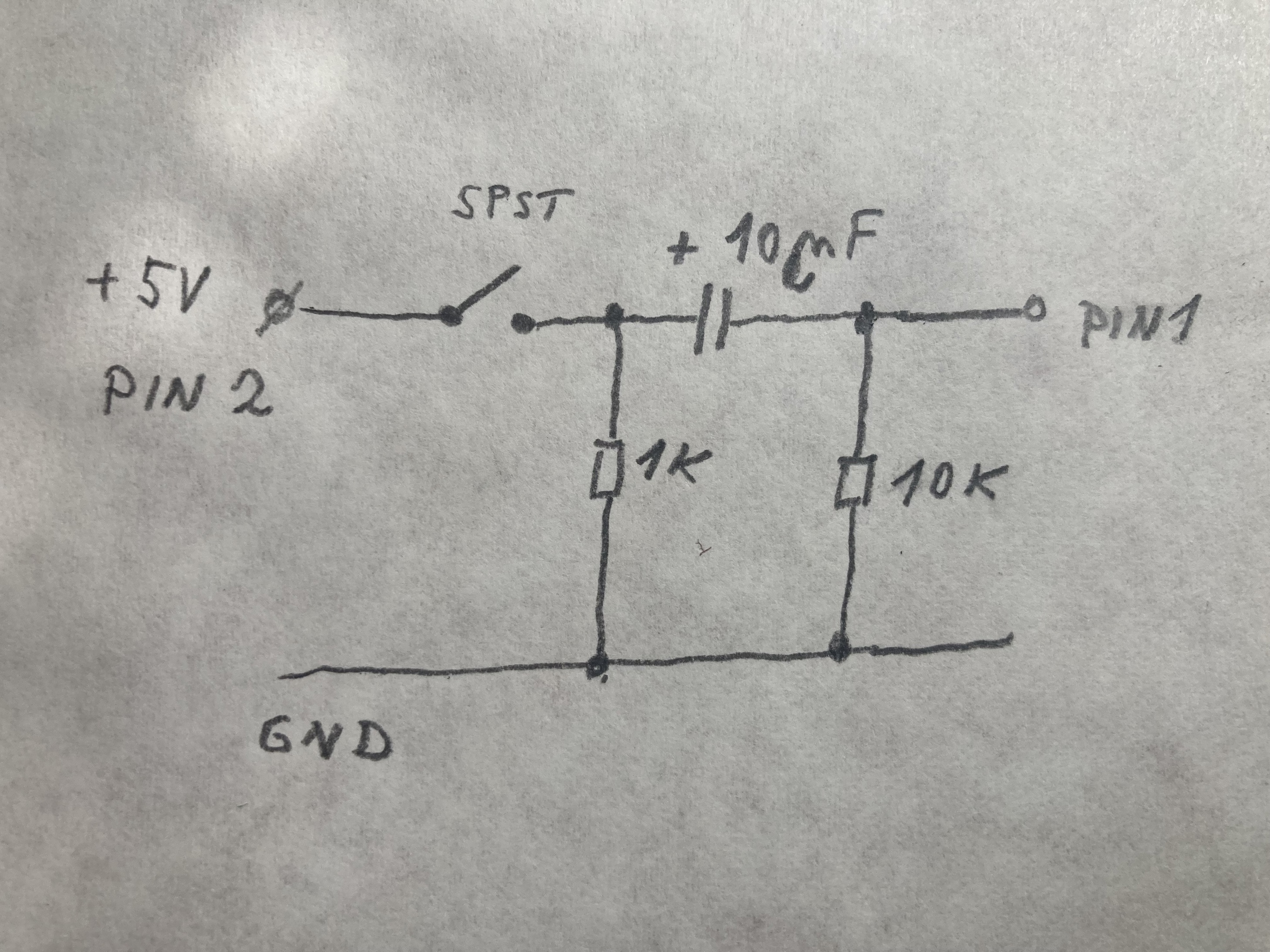
You can replace push-button with Spst according schematic: enter image description here

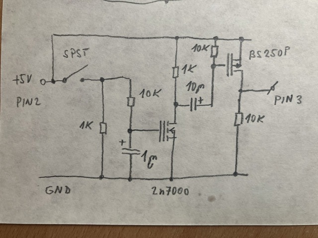
Edit: For pin3 be delayed a little after pin1 use this schematic:

enter image description here

So for pin1 use first schematic and for pin3 use second one. Both are feed from one Spst (right pin).

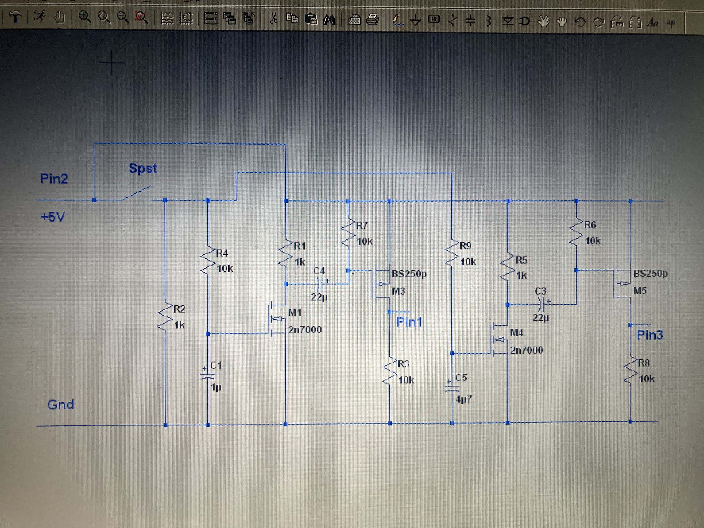
Edit 2: To make it more professional with switch bounce filtering and sharpening/squaring the output edges use this: enter image description here

\$\endgroup\$
9
  • \$\begingroup\$ Thanks, but what's with pin 3? Is it the bottom right line? \$\endgroup\$ Commented Aug 16 at 13:44
  • \$\begingroup\$ The bottom line is Gnd. For pin3 it depends if it needs to be delayed after pin1. If not just use two of this circuits. If yes you need to make a delay with transistors. \$\endgroup\$ Commented Aug 16 at 13:51
  • \$\begingroup\$ Two of this circuit with one SPST? \$\endgroup\$ Commented Aug 16 at 14:00
  • \$\begingroup\$ Yes. Both circuits connect to right side of Spst. \$\endgroup\$ Commented Aug 16 at 14:03
  • \$\begingroup\$ Like I said: Pin 1 + 2, then 2 + 3 and then there shouldn't be any voltage on 1 and 3. But with a single SPST switch this wouldn't work? \$\endgroup\$ Commented Aug 16 at 14:09

Your Answer

By clicking “Post Your Answer”, you agree to our terms of service and acknowledge you have read our privacy policy.

Not the answer you're looking for? Browse other questions tagged or ask your own question.