4
\$\begingroup\$

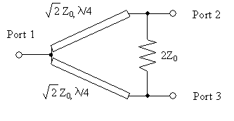
Say we have a Wilkinson power divider:

wilkinson power splitter

The explanation I've heard about how ports 2 and 3 are isolated is this: say there's a signal generator attached to port 2. This can take two paths to port 3: through the resistor, and through the two transmission lines. With the two transmission lines being a half wavelength, they invert the signal. So the non-inverted signal (through the resistor) and the inverted signal (through the transmission lines) is equal but opposite and so cancels.

That makes sense, but it's not enough to convince me that it actually works. For example, why split in half and not some other ratio which would not result in complete cancellation? And wouldn't port 1 have some significance to the operation?

\$\endgroup\$

2 Answers 2

5
\$\begingroup\$

Microwaves101 provides a good qualitative and intuitive explanation, and you seem to understand the idea. For a more rigorous derivation of the scattering matrix you can read section 7.3 (page 328) of Pozar's Microwave Engineering. In this case he uses what is called Even-Odd mode analysis, which he explains pretty well since it is the first time it is used in the text.

For example, why split in half and not some other ratio which would not result in complete cancellation?

The whole idea of the circuit is that it has the property that ports 2 and 3 are 180 degrees away (through the microstrips) and also 0 degrees away through the resistor. This circuit is the simplest way to achieve this property.

And wouldn't port 1 have some significance to the operation?
Yes. The circuit is only lossless if all ports are matched. If there are unequal voltages at ports 2 and 3 at any time power will be lost in the resistor. Assuming all ports are matches, this means the circuit can divide a signal losslessly (because the V2 and V3 will be equal and in phase) and can combine identical & in phase signals losslessly. It cannot combine independent signals losslessly*. This makes them a good candidate for use in solid state RF power amplifiers.

*It is impossible to construct a three-port lossless reciprocal network that is matched at all ports in general.

\$\endgroup\$
6
  • \$\begingroup\$ I guess my confusion is not about how the ports are 180 degrees away, but why they are also equal in magnitude. Is there an explanation somewhere between the very simple and incomplete explanation, and a textbook? \$\endgroup\$
    – Phil Frost
    Commented May 19, 2016 at 19:59
  • \$\begingroup\$ Assume there is very little loss through the microstrip (If the frequency isn't too low this is a good assumption). Input a signal with amplitude A into port 2. At one instant port 2 will be at +A volts, and port 3 will be at -A volts. \$\endgroup\$
    – Andrew W.
    Commented May 19, 2016 at 21:52
  • \$\begingroup\$ The center of the resistor is at 0 volts so port 2 or 3 would see 1*Z0 in shunt to ground looking into the resistor. Half of the input power is dissipated in the resistor and the other is delivered to port 1. In reality there is some finite phase delay through the resistor. You also would never intentionally inject signal at ports 2 without the same signal being injected into 3 as done in the SSPA I linked above. \$\endgroup\$
    – Andrew W.
    Commented May 19, 2016 at 21:58
  • \$\begingroup\$ I think I can see that the center of the resistor is at 0 volts, which would explain why port 2 sees a Z0 impedance, the resistor being twice that. But wouldn't port 2 also see the source impedance of port 1? Wouldn't that change the impedance to ground that port 2 sees? Why in particular does port 1 need to have a Z0 source impedance for this to work? Or is that wrong? \$\endgroup\$
    – Phil Frost
    Commented May 20, 2016 at 1:49
  • \$\begingroup\$ Be careful with terminology, we've been discussing a signal source (generator) at port 2, not port 1. Remember your smith chart. Starting at Z/2 (port 1 || with the leg to port 3) and moving lambda/4 towards the generator (port 2) you will see an open. This means port 2 will only 'see' the Z presented by the resistor. If that's not clear I can create some drawings. It's always hard to talk about this without drawings... \$\endgroup\$
    – Andrew W.
    Commented May 20, 2016 at 5:16
1
\$\begingroup\$

I haven't worked out all of the math details, but I think it's going to be possible to show that if power is injected at Port 2, half of it flows through the resistor toward Port 3, and half flows down the transmission line to Port 1.

At Port 1, this power divides further, sending 2/3 of it out Port 1, and the other 1/3 down the other transmission line to Port 3.

At Port 3, the power through the resistor is attenuated by voltage divider action against the net impedance at that port. The power through the transmission line is transformed in impedance and goes through a similar voltage divider action when it arrives at Port 3, but since it has been delayed by 180° it cancels the resistor power.

Again, I haven't written out the full equations yet, but it seems like it should work out.

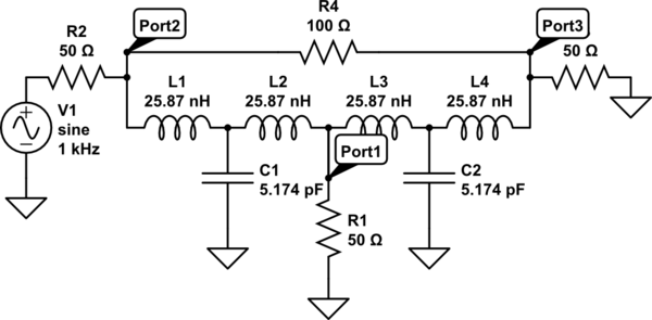
In any case, this simulation shows the effect rather clearly. Just for variety, I used T networks (rather than your π networks) as transmission line simulators. The component values were selected to have reactances of 70.71 Ω at 435 MHz. There is a deep dip in the power delivered to Port3 at that frequency, and equal amounts of power are being dissipated in R1 and R4.

schematic

simulate this circuit – Schematic created using CircuitLab

\$\endgroup\$
3
  • \$\begingroup\$ Dave, I agree with everything you said except for a clarification. You say "... if power is injected at Port 2, half of it flows through the resistor toward Port 3..." Half the power is delivered to the resistor, BUT it is delivered in both directions since there is voltage on either end of the resistor. \$\endgroup\$
    – Andrew W.
    Commented May 19, 2016 at 23:30
  • \$\begingroup\$ @AndrewW.: I hope we're not talking past each other here because of a confusion in terminology. The current through the Port1-Port3 transmission line exactly matches the current through the resistor (R4), so there is not in fact any voltage at Port3. \$\endgroup\$
    – Dave Tweed
    Commented May 19, 2016 at 23:42
  • \$\begingroup\$ I believe we are. No power leaves port 3 because the voltage across the resistor (R4 in your schematic) cancels with the voltage wave initiated from port 2. \$\endgroup\$
    – Andrew W.
    Commented May 20, 2016 at 4:56

Your Answer

By clicking “Post Your Answer”, you agree to our terms of service and acknowledge you have read our privacy policy.

Not the answer you're looking for? Browse other questions tagged or ask your own question.