0
\$\begingroup\$

I understand that up until a point (Vforward), the differential resistance is positive. And then it turns negative, and as the voltage increases, the current decreases, as you can see in this IV curve for a PCT (Point-Contact Transistor):
iV curve PCR

One can see that up until the red shaded region that the object acts as a normal resistor, where more volts will get you more current. Simple thus far. Next, in the shaded region, one can see that as you apply more volts, less current passes through the device, which inclines me to believe that something must be working "against" the voltage, and that this is acting as a generator that opposes the voltage direction.

But what physical phenomena can explain this?

How does it work with respect to electric fields, currents, and material types for a Point contact transistor?

\$\endgroup\$
10
  • \$\begingroup\$ Can you provide a I-U diagram or a datasheet? \$\endgroup\$
    – Simon
    Commented Sep 27, 2016 at 20:30
  • \$\begingroup\$ @Simon working on it \$\endgroup\$
    – user86234
    Commented Sep 27, 2016 at 20:32
  • \$\begingroup\$ What is your background? Are you familiar with the Schrödinger equation? \$\endgroup\$ Commented Sep 27, 2016 at 21:45
  • \$\begingroup\$ "Under normal forward bias operation, as voltage begins to increase, electrons at first tunnel through the very narrow p–n junction barrier and fill electron states in the conduction band on the n-side which become aligned with empty valence band hole states on the p-side of the p-n junction. As voltage increases further, these states become increasingly misaligned and the current drops" - Wiki \$\endgroup\$
    – jbord39
    Commented Sep 28, 2016 at 0:37
  • \$\begingroup\$ @AndrewSpott somewhat familliar.. \$\endgroup\$
    – user86234
    Commented Sep 28, 2016 at 1:37

3 Answers 3

0
+50
\$\begingroup\$

This is something that I have been spending some time looking into over the past few hours, with luck the answer will be coherent. If something needs clarification, I will be happy to try my best.

edit: I just noticed that you are talking about point contact transistors. I'm not familiar with these devices, and so I don't know much about them. The following discusses tunnel diodes.

In quantum mechanics, the double barrier potential describes a system where there are two potential barriers to overcome for a particle to get through the system. This potential is a very simple picture what an electron will see in a resonant-tunneling diode:
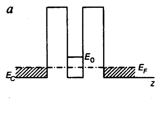
Double barrier potential

Where \$E_F\$ is the fermi level of the semiconductor (see below), \$E_C\$ is the conduction band energy level (the lowest energy level occupied by electrons in the conduction band), and \$E_0\$ is the minum energy level band within the double barrier. The higher energy level bands within the double barrier can be labeled \$E_1\$ through \$E_n\$, and will be approximately quadratically space (\$E_n - E_{n-1} ∝ n^2\$). The conduction band will go from \$E_C\$ to \$E_F\$ (at zero temp).

Here, we need to talk about density of states. The figures shown are only for a single direction in space. For the other two directions, the momentum is less confined. The total momentum of an electron is:

$$ p_x^2 + p_y^2 + p_z^2 \leq 2mE_F $$

For the energy band \$E_0\$, the momentum can be:

$$ p_x^2 + p_y^2 + p_z^2 \in 2mE_0 $$

There are two things that are necessary in order for the electron to tunnel: 1) the energy that it starts with, and the energy that it ends with must be the same. 2) the momentum in the \$z\$ direction that the electron starts with and ends with must be the same.
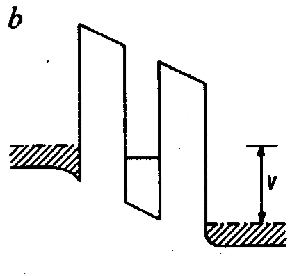
biased double barrier potential

Initially as the bias voltage is applied, only electrons at the fermi level will be able to transition over. When this is the case, all the energy of the electron will be in the \$z\$ direction (\$p_x=p_y=0\$). As the bias voltage increases, more \$p_x\$ and \$p_y\$ states will be able to tunnel (\$p_z\$ will get smaller), hence increasing the current, hence a positive resistance (more voltage = more current). As the voltage bias continues to be increased, the energy of \$E_0\$, relative to the fermi level on the left \$E_F\$ decreases.

When \$E_0=E_C\$, only \$p_z=0\$ electrons can tunnel through, and for higher bias voltages than this, electrons must tunnel through both barriers in order to flow. However, with continued increase in the bias voltage, the higher energy levels of the double barrier potential \$E_1\$ will get close to \$E_F\$ allowing this process to continue (this time through \$E_1\$ rather than \$E_0\$). This leads to the positive differential resistance again.

This picture gets fuzzier at temperatures higher than 0 K. Lattice vibrations and temperature effects make this cutoff fuzzy, rather than sharp, leading to negative differential resistance.


Aside: The fermi energy can be though of in a couple of different ways, but for our purposes, I'm going to think about it this way: At zero temperature, this is the energy level of the highest occupied energy level of the solid. At non-zero temperature, there is some distribution of occupied energy levels above $E_F$ due to thermal energy being given to the electrons. This distribution decreases as you get to higher energy above the fermi energy. These electrons have to come from somewhere, so the energy levels occupied below the fermi level also decrease.


See: http://www.ece.sunysb.edu/~serge/67.pdf for a decent "review article" in Nature.

\$\endgroup\$
8
  • \$\begingroup\$ for this explanation, i'm assuming the Z-Axis is "through", right? \$\endgroup\$
    – user86234
    Commented Sep 28, 2016 at 14:10
  • \$\begingroup\$ Correct, z is through the device. \$\endgroup\$ Commented Sep 28, 2016 at 14:20
  • \$\begingroup\$ So, If I'm getting this correct, In order to tunnel, the momentum in must be equal to momentum out, thus the power dissipated by the electrons (P = IV) is staggered to be proportional (more or less) to the difference between the fermi and the minimum energies? $$P\propto E_{0}-E_{f}$$ \$\endgroup\$
    – user86234
    Commented Sep 28, 2016 at 15:32
  • \$\begingroup\$ This is a little weird, because on the right side of these figures, we are high in the conduction band: approximately vbias higher than we started. There are lots of unoccupied states below this state, and so the electron drops energy levels, in the process releasing energy as heat/light/etc. So your equation is right for the fermi level on the right side of the double barrier. \$\endgroup\$ Commented Sep 28, 2016 at 15:43
  • 1
    \$\begingroup\$ I didn't mention it in the original post, I've edited it to make that more clear, and I'll add more about the return to positive differential resistance in a sec. E_1 is the second energy level of the double barrier (the double barrier can support a number of energy levels). The process can continue with a PDR then NDR, then PDR, then NDR until you run out of energy levels within the double barrier, however I believe that there are "real material" effects that limit this somewhat \$\endgroup\$ Commented Sep 28, 2016 at 16:06
1
\$\begingroup\$

enter image description here

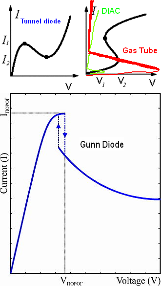
Let's discuss two types of negative differential resistance ( out of 4)

A) a forward voltage causes current to rise quickly like a hot resistor but due to special Fermi Levels in a semi-conductor, a threshold is reached resulting in current to drop abruptly which follows the same path back with some hysteresis.

  • example is the Gunn Diode for extreme high microwave resonators

B) A forward voltage occurs with little or no current until a threshold is reached and then the voltage collapses to a low voltage and then rises like a resistor with more voltage and current.

  • example is a DIAC which is used to trigger SCR's , ( "somewhat" similar to a 3 leaded Unijunction and SCR characteristics except with 2 leads.)

  • example gas tube ( neon, transient suppressor, fluorescent , air arc (ESD) corona, etc) these have much high trigger levels which is sensitive to gas pressure and vacuum. In air BreakDown Voltage (BDV) that is 1kV/mm to 3kV/mm

    • Here a dielectric gas, which is an insulator, excites electrons under an electric field until the the electrons escape the outer orbit, and depending on the gas and current may emit X-Rays like FL tubes which hit the phospors inside glass and secondary electron emission results in a lower visible wavelength and conducting lots of ions which drops the voltage as current rises with a -ve R.
\$\endgroup\$
-4
\$\begingroup\$

Simple resistances don't have negative differential resistance:

https://en.wikipedia.org/wiki/Negative_resistance

Only specific devices show such behavior in a limited range
for device like

https://en.wikipedia.org/wiki/Tunnel_diode

the explanation is a large dose of quantum physics

\$\endgroup\$
6
  • \$\begingroup\$ I read the wiki page, but it mentions little of what happens in relation to electric fields. \$\endgroup\$
    – user86234
    Commented Jul 20, 2016 at 18:26
  • 1
    \$\begingroup\$ That does not answer the question at all. \$\endgroup\$
    – jbord39
    Commented Sep 27, 2016 at 20:51
  • \$\begingroup\$ @jbord39 I would like to see your simple explanation of Tunnel Diode behaviour without using a lot of quantum physics. \$\endgroup\$
    – matzeri
    Commented Sep 27, 2016 at 21:04
  • \$\begingroup\$ @matzeri: "Tunneling diodes work because of quantum tunneling. The charge carriers are thus described with a probability distribution rather than as single co-ordinate in space. This distribution looks like a normal distribution in most cases. Since the distribution can tail off through the insulating oxide, there is a finite chance that an electron will show up on the other side. Because this is a statistical process in nature, it is very easily calculated at which rate this will occur on a macro-scale." Obviously hand wavey but at least mentions the concepts. \$\endgroup\$
    – jbord39
    Commented Sep 27, 2016 at 22:00
  • 1
    \$\begingroup\$ @matzeri: On top of that, he asked for the explanation. Regardless of whether or not I can give this explanation is irrelevant, beacuse I did not attempt an answer. You did attempt an answer, and it is a very poor answer at that, since you explain nothing that he asks. Your straw-man argument (asking me to explain quantum tunneling without quantum mechanics) is irrelevant to his questions, because he DOES ask for an explanation of the behaviour, which your answer wholly fails to provide. \$\endgroup\$
    – jbord39
    Commented Sep 27, 2016 at 22:02

Your Answer

By clicking “Post Your Answer”, you agree to our terms of service and acknowledge you have read our privacy policy.