3
\$\begingroup\$

This is not a sourcing question; I don't need part numbers or manufacturers.

Most DC/DC converters (LDO, buck, etc) with an adjustable output voltage have you set that voltage using a resistor divider or equivalent. The divider takes the output voltage and ground and uses them to produce a feedback voltage.

If the output voltage needs to be (digitally) adjustable, then the resistor divider needs to be adjustable too. The most straightforward way of doing this is to have one half of the divider be a digital potentiometer (digipot) or digital rheostat. The problem here is that even in large quantities (>3000 units) digipots are very expensive -- even the cheap ones are around $0.40 in large quantities, which can be more than the inductor or even the regulator!

Is there some trick for achieving an adjustable output regulator without needing this expensive component? Technically a digital resistor is overkill since (if you make the low-leg of the divider the programmable one) you know that one side of the resistor is always at ground. So I've looked into digitally adjustable current sources but they seem to be pricey too.

Also, in my particular situation absolute accuracy is not terribly important; I can accept the regulator voltage output being wrong by as much as 10-20% (there's enough headroom to avoid damaging other components). The fine adjustment of the voltage output (down to ~1%) is then done by a software feedback loop that seeks out the maximum operating frequency of the rest of the system at a particular voltage and then finds the optimal voltage=power/performance tradeoff. So I don't need the output at exact X volts, just X+/-20% and then the ability to nudge it up or down by ~1%.

\$\endgroup\$
8
  • 1
    \$\begingroup\$ Smoothed PWM and a FET? \$\endgroup\$ Commented Jul 26, 2016 at 22:59
  • 1
    \$\begingroup\$ @IgnacioVazquez-Abrams, Are you answering from experience? I haven't tried it (and I have a similar design problem on my plate to OP's), but I'd be concerned about the smoothing filter adding delay in the control loop. \$\endgroup\$
    – The Photon
    Commented Jul 26, 2016 at 23:14
  • \$\begingroup\$ @Ignacio, using the FET gate as a capacitor as the integrator? I'd thought of using capacitors to integrate PWMs but this is for a buck converter which (at this early prototyping stage) has really awful EMI emissions (those get cleaned up once everything else works). I'm a bit nervous about having any nodes that aren't strongly driven lying around. \$\endgroup\$
    – user4718
    Commented Jul 26, 2016 at 23:18
  • 1
    \$\begingroup\$ You could build around a programmable converter IC: linear.com/products/digitally_programmable_regulators - or you could just build your own programmable buck from a microcontroller. \$\endgroup\$
    – pjc50
    Commented Jul 27, 2016 at 11:26
  • 1
    \$\begingroup\$ @pjc, those cost a lot more than digital rheostats. not really helpful. \$\endgroup\$
    – user4718
    Commented Jul 28, 2016 at 2:16

5 Answers 5

2
\$\begingroup\$

It's really hard to do this with a generated voltage without degrading the voltage accuracy of the regulator.

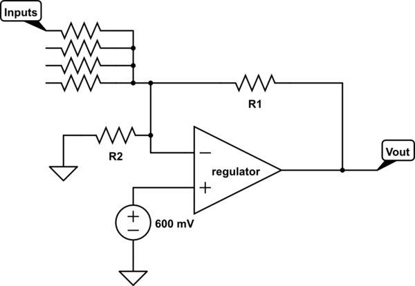
But if you have a handful of digital outputs that you can dedicate to this, you can use a resistor digital-resistance-converter (DRC?) like this. I've represented the regulator as an op-amp.

schematic

simulate this circuit – Schematic created using CircuitLab

The four trim resistors are switched out of the circuit by setting microcontroller pins to inputs and they are switched into the circuit by setting microcontroller pins as digital output lows.

When all four pins are inputs, the voltage divider is R1 and R2. When some pins are set, the divider is R1 and the parallel combination of R2 and the trim resistors.

I would suggest setting the lowest voltage with R1 and R2, the select the trim resistors to pull the voltage over the range that you want. Do not choose all four resistors the same value. Instead you will want something like a 1k,2k,4k,8k sequence so you can get 16 different values out.

For extra credit:

  • If your microcontroller has switchable high-side outputs (open-drain) you can do that instead of switching input to output, then
  • If your microcontroller has outputs as bits in a PORT register, arrange the resistors with the largest value on the least-significant output bit. Then with careful resistor value choice, you can write 0-15 to the port register to get monotonically increasing voltage.
\$\endgroup\$
3
  • \$\begingroup\$ isn't this just building a DAC out of discrete components? \$\endgroup\$
    – user4718
    Commented Jul 28, 2016 at 2:18
  • \$\begingroup\$ FWIW I did at one point consider doing this with a 74HC595. Those cost about 5x less than the cheapest DAC or digipot (resistors are basically free) and one of them gets you 8-bit resolution from one GPIO pin. And you can daisy-chain them. \$\endgroup\$
    – user4718
    Commented Jul 28, 2016 at 2:20
  • \$\begingroup\$ This is not a DAC because the change is in resistance, not voltage. Therefore, no other reference voltage appears in the formula for output voltage. If you use a '595, it needs to be an open-collector one like TPIC6B595 \$\endgroup\$
    – markrages
    Commented Jul 28, 2016 at 4:18
2
\$\begingroup\$

What you are describing is voltage margining. (I am not suggesting using the DAC in the app note).

Russell is suggesting almost this, I think.

The advantage to margining is that it is not the primary voltage setting element, so if that fails, then the output will still be within some reasonable (calculated) percentage of nominal Vout.

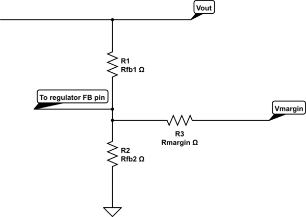
A simple margining circuit (that will not typically interfere with loop compensation) starts with this approach:

schematic

simulate this circuit – Schematic created using CircuitLab

The key here is Vmargin. It is an analogue source (easily achievable from PWM and a filter); note that the filtering of Vmargin using a capacitor will be isolated from the feedback loop by Rmargin.

The design equations are quite simple:

\$V_{OUT(NOM)}\ =\ V_{FB} \cdot \left( 1\ +\ \frac {R_{fb1}} {R_{fb2}} \right)\ + \ I_{FB} \cdot R_{fb1}\$

\$V_{OUT(MIN)}\ = \ V_{OUT(NOM)} - \frac {R_{fb1}} {R_{margin}}\ \cdot \left(V_{margin(max)}\ - V_{FB} \right)\$

\$V_{OUT(MAX)}\ = \ V_{OUT(NOM)}\ + \ \frac {R_{fb1}} {R_{margin}}\ \cdot \left(V_{margin(min)}\ + V_{FB} \right)\$

This assumes that the source impedance of Vmargin is << Rmargin.

Rmargin is usually much larger (2.5:1 or so) than either feedback resistor. Other answers have suggested methods of achieving an inexpensive analogue source suitable for Vmargin.

I think the addition of a single resistor with an inexpensive analogue source might meet the cost criteria you require.

[Update]

I think using your concept of a 74HC595 as a resistor programming chain for a summing junction that is then buffered to provide Vmargin may be a low cost solution for the analogue voltage source.

\$\endgroup\$
3
  • \$\begingroup\$ This is a very good explanation and approach. I would suggest a N-FET transistor as a variable resistor element in the "Vmargin" branch of the above circuit, which will provide better isolation from PWM-style DAC. Or just a normal DAC. Something like a light 2N7002, to have smaller channel capacitance. The control path can be calibrated, so the set-up voltage can be controlled with decent quality. However, the DAC/PWM channel will also have some cost, as compared to a I2C link to a digital trimpot. \$\endgroup\$ Commented Jul 27, 2016 at 17:40
  • \$\begingroup\$ Hi Peter, the last rev of my board actually has exactly this circuit although I didn't know it had a name ("voltage margining"). It is cool and useful but does not really solve the problem at hand: the problem is just moved from generating a resistance to generating an analog voltage. I had vmargin driven by an opamp and then just sorta went hurr durr and disabled the opamp because I couldn't figure out a cheap way to control it digitally :( \$\endgroup\$
    – user4718
    Commented Jul 28, 2016 at 2:26
  • \$\begingroup\$ But you raise a good point here: by making Rmargin much larger than the other two resistors you sacrifice range but also minimize the impact of any noise on Vmargin. So this, combined with a filtered PWM, appears to be the best answer yet. If nothing better comes up I'll accept yours (with honorable mention to @Ignacio Vazquez-Abrams comment, which was the first to mention PWM). But really I was kinda hoping there was some better trick out there; I guess there isn't unfortunately. \$\endgroup\$
    – user4718
    Commented Jul 28, 2016 at 2:28
1
\$\begingroup\$

Is there some trick for achieving an adjustable output regulator without needing this expensive component?

Summary:

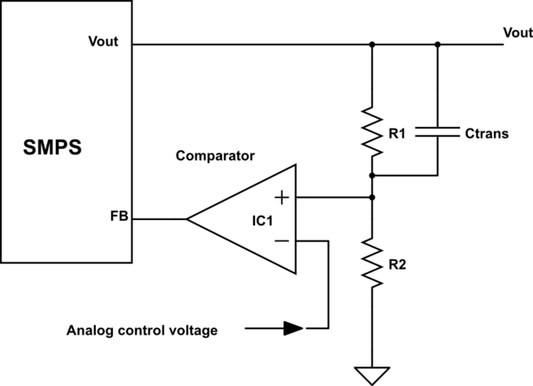
Instead of Vout being divided and used to drive a feedback input pin Vfb,
an external comparator is used to compare the divided Vout voltage with a user generated analog signal. The comparator output then drives Vfb

While there may be some applications where this approach is inappropriate,
in practice the method usually works well when applied intelligently.

Basic principle - outline only:

'SMPS' is existing power supply control IC.
'FB' is feedback voltage input. Originally: R1, R2 divide Vout so voltage at pin FB = Vref_internal when Vout is desired voltage.

IC1 (opamp or comparator) is added in the feedback path so that now Vout divided is compared with the supplied control voltage. When Vout rises above desired level Vfb is driven high, exceeding internal Vref. When Vout is below desired level Vfb is low.

Bonus: I've shown a capacitor, Ctrans, in parallel with R1. This is often not included in designs but is often useful or very useful. Functionality can be analysed formally, but can be thought of as adding a high-pass boost to the feedback signal or as coupling Vout transients to the feedback pin with decreasing loss as transient rate of change increases. This has the effect of causing the system to respond more rapidly to transient changes, such as load increase/decrease or noise on the supply rail from other sources (which can be considered to be load changes). Too large a value of Ctrans is an invitation to disaster but somewhere in the 10pF-1nF range will often be appropriate.
schematic

simulate this circuit – Schematic created using CircuitLab

__________________________________________

Detail:

When a variable pot is used the system compares the divided output (input on pin "Vfb") with a reference voltage Vref, often supplied from inside the control IC, and makes suitable decisions (usually on/off switching transitions).

The same conceptual result can be achieved by comparing the divided output voltage with a user variable voltage derived by other means (usually with an external comparator or opamp). The result of the comparison is then used to "inform" the control IC in place of the usual divided Vout input (typically called something like Vfb = Vfeedback). While the expectation is that the system will be maintained with Vfb adjusted by the controller to remain at Vref_internal, feeding an on/off signal from an external comparator usually achieves much the same result.<2> Most smps IC's deal with the fb pin being above or below Vref_internal either on a cycle by cycle basis or terminate the current cycle if Vfb rises above Vref during a cycle.

One way to provide the external user adjustable analog signal is to generate a PWM signal and filter it to provide an analog voltage that varies in proportion to the PWM mark-space ratio and the PWM maximum and minimum voltage levels.

ie Vanalog ~~= V_PWM_min + V_PWM_max-VPWM_min) x dc

where dc is the fractional on duty cycle. Usually Vmin is ground and Vmax is the maximum output level of a processor pin or gate - typically ~= Vdd.

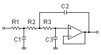
Now, the desired voltage can be set using PWM at the cost of one processor or other pin and some analog filtering. If available an analog DAC output could be used. If response time is not crucial then a single pole RC filter (Rout-series followed by a capacitor to ground)will often provide enough filtering to prevent the output following the PWM related analog ripple. If faster response is wanted then a simple multipole analog filter can be used. A 3 pole low pass filter can be achieved with a single low co opamp section (1/4 quad package) and typically 3 resistors and 3 capacitors. This is still significantly lower cost than a digital pot in most cases.

__________________________________

Digipot pricing:

A check on Digikey showed that their lowest cost digipot the MCP41\01x was $US0.39 in 3000+ quantity - right on the price point suggested. I'd expect the cost in volume production in China to be significantly lower than that. I've never priced digipots in China but I'd expect something in the $US0.10-0.15 range.

__________________________________

Low pass filter design

"Bearably good" low pass filters can be achieved using emitter followers as unity gain stages. Thus, a 3 pole low pass can be achieved with a "jellybean" transistor<1>. The main disadvantage is the Vbe offset voltage which makes Vout_DC less determinate. With the stated 20% requisite precision the Vbe drop can probably be adequately allowed for by suitable design assumptions. If an ADC input is available to measure Vref_DC OR the final output voltage then the offset is not a problem.

Many design aids for low pass (and other) filters are available.
These are just a small sample.

Possibly the most usefil topology - many implementations achieve two low pass poles per gain or buffer stage but it is possible to achieve 3 poles on the first stage using a Sallen & Key design with unity gain buffer.

This site 3rd order Sallen-Key Low-pass Filter Design Tool provides a calculator to implement this circuit with a useful range of output analyses provided.
enter image description here

EDN doing similar with theory added.
Design second- and third-order Sallen-Key filters with one op amp

Active Filter Design Techniques 66 pages

Useful?:

http://www.electronics-tutorials.ws/filter/filter_8.html

https://en.wikipedia.org/wiki/Low-pass_filter

Here is the usual large range of potential webpages via image serach using key: 3rd order active low pass filter

TI 2002 SLOA0409B 24 pages. Only uses 2 poles per opamp section.
Active Low-Pass Filter Design

_______________________

Response to an objection to this proposal:

This is added as part of the answer as it serves to 'explain' various aspects of the method. I've added notes <1> etc to my answerabove to allow ease of reference.

IMO, the suggested "solution" makes no sense.

The solution can be (and almost invariably will be) far less complex than you suggest.
It is one standard way of achieving the aim and it can often be made to work entirely well in practice.
All potential 'solutions' to any problem need to be evaluated for 'goodness' using whatever parameters are relevant in each case.

A continuously-running PWM

Yes, or other analog source. Often easily enough provided as a processor funtion or in software

OPAmp to filter the PWM to DC

Yes, or as above a jellybean bipolar emitter follower - see <1> above.
Cost of bipolar ~= 1 cent US in Chinese modest production, + 3R +3C .

Then I guessyou will need another OPAmp to provide the level shift of new biased signal into feedback pin of PMIC ...

No. Not usually. See <2> Opamp rail-rail signal can usually be used.
This can be limited or clamped or shaped but often used as is.

... plus a dozen of passive components, likely two power rails (+V, -V).

No. the components mentioned are often enough as is. Power rails are liable to be just Vdd and ground and already used to supply an opamp which a 1/4 or 1/2 of is available in. If a bipolar transistor is used no explicit power supply is needed other than what is already in use.

Plus all corresponding PCB space.

PCB real estate is always required for hardware. Here a 1/4 pkg op amp may be available. 3 Rs and 3 Cs at smallest acceptable pkg size are liable to suffice. An external digipot would probably require similar PCB area (say 6 lead pkg) or maybe slightly less depending on whether and existing 1/4 pkg opamp is free and whether the digipot neded any support components. It also may need routing of 2 or 3 signal leads depending on protocol and power routing. Overall it's reasonable to assume they are about the same area wise without specific information.

you have any BOM estimation in mind,

Comparing apples with apples and using digikey 3000 pricing, an LM324 costs $0.09 in an SO pkg or $0.099 in a TSSOP or QFN16 . So if you have to but the whole quad, 10 cents for the pkg of 4 or 2.5c per opamp, or free if it's spare. Single opamps can be had in pkgs small enough to risk being a breathing hazard [ :-) ] but cost is no better or worse.

not speaking that extra OPA will change transfer function of PMIC feedback loop and potentially cause instability or alter dynamic properties of the voltage regulator?

Potentially, yes. As above - "All potential 'solutions' to any problem need to be evaluated for 'goodness' using whatever parameters are relevant in each case.". Changing circuitry in a feedback loop matters. In SOME cases the above solution may cause more problems than it solves, However, the good news is that in many cases it works well. An error amplifier / comparator exists inside the smps IC - we are effectively extending it externally. If the internal amplifier acted on the difference between reference and feedback signal then replacing the signal with a high/low signal may well affect operation. But the very large majority of smps ICs use the feedback input to trip a go/no-go internal operation - usually latched on a cycle by cycle basis. "It usually works well when applied intelligently" is a good starting point.

\$\endgroup\$
4
  • \$\begingroup\$ Hi Russell, thanks for your comment. Regarding PWMs, are you proposing something other than a capacitor as an integrating element? If so, see the noise concerns I raise in comment above. Regarding DACs, this would be great, but aren't DAC chips even more expensive than digital rheostats? The opamp suggestion is intriguing, we're already buying those in massive quantities and get great prices (and might even have half of a dual opamp lying around unused for free). Can you point me to a schematic or a search term that would lead me to one? \$\endgroup\$
    – user4718
    Commented Jul 26, 2016 at 23:21
  • \$\begingroup\$ @user4718 See additions to answer re filters. | I mentioned DAC meaning in-processor - usually not available or in short supply. What is the overall design doing, if I may ask? \$\endgroup\$
    – Russell McMahon
    Commented Jul 26, 2016 at 23:50
  • \$\begingroup\$ So what do we have here? You are suggesting (a) a continuously-running PWM controller; (b) OPAmp to filter the PWM to DC, then I guess you will need another OPAmp to provide the level shift of new biased signal into feedback pin of PMIC, plus a dozen of passive components, likely two power rails (+V, -V). Plus all corresponding PCB space. Do you have any BOM estimation in mind, not speaking that extra OPA will change transfer function of PMIC feedback loop and potentially cause instability or alter dynamic properties of the voltage regulator? IMO, the suggested "solution" makes no sense. \$\endgroup\$ Commented Jul 27, 2016 at 0:08
  • \$\begingroup\$ @AliChen I've addressed your various points in an addition to my answer. In summary: It works well in many cases, cost can be very low - it can use a spare OA if available OR just a <= 1 cent transistor & 3 x R, 3 x C (as in answer). Extra OA and components are most unlikely to be needed. See details in answer. \$\endgroup\$
    – Russell McMahon
    Commented Jul 27, 2016 at 17:02
0
\$\begingroup\$

The tactic that Dave Jones (EEVBlog) took in designing a Lab power supply (part1, part2) was to use an op-amp to set the control voltages, and the micro-controller's output (PWM??) pins would be used to control the op-amps. I don't recall the exact reasons for his methodology though.

As far as I know, a reference circuit generally is an example; i.e. a good starting point for designing and/or learning about the chip. The data sheet containing the reference circuit should have some indication as to what is required to make the chip work and what is there as tune-able parameter. is the voltage-divider required as a feedback mechanism, or is simply to set the control voltage?

\$\endgroup\$
6
  • \$\begingroup\$ is the voltage-divider required as a feedback mechanism, or is simply to set the control voltage? both \$\endgroup\$
    – user4718
    Commented Jul 27, 2016 at 2:59
  • \$\begingroup\$ The Dave Jones power supply is a confused design and should not be used as a power supply design guide. More comments at reddit.com/r/AskElectronics/comments/2o5fmt \$\endgroup\$
    – markrages
    Commented Jul 27, 2016 at 4:40
  • \$\begingroup\$ The Dave Jones supply controls one of LT's 'new generation' current controlled linear regulators (whose method of operation is not the same as eg 7805 type regulators even though the circuits may look similar at a glance. While his general method is OK some of the circuitry needs to be altered for more traditional voltage feedback control. Some of the Reddit comments may be true but not excessively important in the context. \$\endgroup\$
    – Russell McMahon
    Commented Jul 27, 2016 at 11:42
  • \$\begingroup\$ The design is unfinished, so maybe Dave will converge on a better design if he ever tries to get it working. There are just some mistakes in the design as it is now, which makes it a bad choice to learn from. \$\endgroup\$
    – markrages
    Commented Jul 27, 2016 at 16:41
  • \$\begingroup\$ @markrages looks like I might have linked the wrong set of episodes, iirc he did build it, but changed a bunch by the end. \$\endgroup\$
    – esoterik
    Commented Jul 28, 2016 at 1:30
0
\$\begingroup\$

Since you want to digitally control an analog quantity (voltage) it's a clear application for a DAC. Simplest approach is to feed the output of the DAC to the reference input of your regulator. That might not work because some regulators have internal references, or won't take a large common mode range on the reference pin

Alternately, you can set an op amp or two as a summing amplifier, generating

Vout/scale1 + DAC/scale2

and the regulator that gets THAT fed to its sense pin will adjust the voltage to

Vout = scale1*(Vref - DAC/scale2)

Solve for 'scale1' and 'scale2' so that the Vout range is as desired. If some fine-adjust is required, the summing amplifier can take input from any number of other DACs.

\$\endgroup\$
5
  • \$\begingroup\$ DACs are even more expensive than digipots. I can't see how this helps. \$\endgroup\$
    – user4718
    Commented Jul 27, 2016 at 0:48
  • \$\begingroup\$ Low-cost DACs are digipots. \$\endgroup\$
    – markrages
    Commented Jul 27, 2016 at 4:57
  • \$\begingroup\$ A digipot doesn't include a reference voltage, which limits how it can be applied. The combination of an op amp and a DAC solves a number of range-limit issues. \$\endgroup\$
    – Whit3rd
    Commented Jul 27, 2016 at 6:19
  • \$\begingroup\$ Well, this is academic. All digipots and all DACs cost more than $0.40/each in volumes around 3000pcs. \$\endgroup\$
    – user4718
    Commented Jul 28, 2016 at 2:30
  • \$\begingroup\$ Of course it's academic! The conversion of digital to analog, the DAC function, is NOT exclusively accomplished with a standalone chip called 'a DAC'. You can take four CMOS outputs into an R/2R network, and make a DAC for the cost of eight resistors. Or you can use a single DAC for eighteen outputs, with track/hold amps. You aren't stuck paying for a catalog item called 'DAC'. \$\endgroup\$
    – Whit3rd
    Commented Jul 28, 2016 at 20:04

Your Answer

By clicking “Post Your Answer”, you agree to our terms of service and acknowledge you have read our privacy policy.

Not the answer you're looking for? Browse other questions tagged or ask your own question.