My question is to find whether there can be a definitive answer to this particular part.
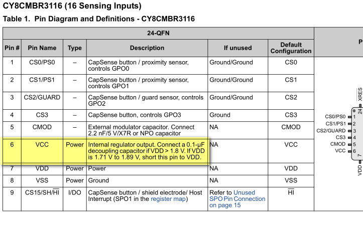
I have Cypress MBR3002 IC which has two power pins labelled VCC and VDD.
I got a question from my colleague about the reason behind two different names for two power pins.
According to datasheet, VDD is actual power pin and VCC is internal to the IC. At lower supply voltage, both needs to be supplied by external supply itself. At higher voltage VDD is internally derived by the IC using external VCC.
I had this great answer about terminologies and I was able to answer on similar lines.
But, I would like to know if there are any good reasons for the labels VDD and VCC in this particular IC only.
Edit: Should I drop this search right now and see other important stuff?


VCC stands for "voltage at the common collector, which imply that CC stands for "common collector". I think that is not how the terminology evolved historically. See this good detective answer delving into a 1965 IEEE standard.. \$\endgroup\$