1
\$\begingroup\$

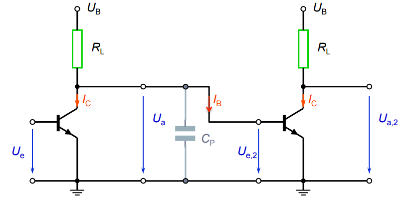
We discussed BJT-transistors in the lecture and this circuit came up, the professor said that this circuit would act as some sort of amplifier for the transimitted signal between the two transistor but I dont understand how it works.

Later I discussed it in a training group and was told that the signal would bounce between the two transistors because of the capacitor, but this confused me even more.

enter image description here

\$\endgroup\$
11
  • 5
    \$\begingroup\$ Nothing is bouncing. Two inverter stages after each other forming a buffer/amplifier of sorts. The first Rl and Cp will form a low pass filter. \$\endgroup\$
    – winny
    Commented Jan 12, 2017 at 20:57
  • 2
    \$\begingroup\$ And the signal to be amplified is connected at Ue point. \$\endgroup\$
    – Golaž
    Commented Jan 12, 2017 at 20:59
  • 3
    \$\begingroup\$ "BJT-Transistor" is redundant (the "T" already stands for transistor) \$\endgroup\$ Commented Jan 12, 2017 at 21:03
  • 3
    \$\begingroup\$ Yes, but BJ sounds rude. So BJT. \$\endgroup\$
    – Ian Bland
    Commented Jan 12, 2017 at 21:05
  • 8
    \$\begingroup\$ The voltage at the collector of the first BJT will be clamped at 0.7V (approx) by the base-emitter junction of the second BJT. BJT(2) is most likely in saturation (so only a small DC output say 0.2V). BJT(1) has no bias arrangement so it impossible to tell what Ue will actually do to BJT(1). (Is Ue a DC or AC or mixed signal? - no one knows. ). Its a terrible example to give to a class who are just learning to come to grips with the basics. I'm not surprised you were confused. \$\endgroup\$ Commented Jan 12, 2017 at 21:19

3 Answers 3

2
\$\begingroup\$

Given your instructor's remark, I suspect that you were actually told about "debouncing", which a very useful function. However, the circuit shown is a bad, bad example of how to do it.

Let's think about a switch making contact. Inside, you have two pieces of metal making contact, and on a timescale of milliseconds the two pieces can actually bounce, perhaps repeatedly, before settling down. If this happens the switch output will apparently show multiple activations where only one was intended. To combat this, a circuit like this can be used:
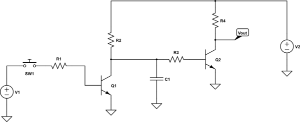
schematic

simulate this circuit – Schematic created using CircuitLab

You've noticed that it has the same general outline as your circuit, but a few more resistors.

Let's say that the switch is open, and gets briefly closed, then open, then closed for good (a single bounce). Current through R1 turns on Q1 and pulls the collector low. This also discharges C1. As a result Q2 is turned off and Vout goes high. When the switch bounces, Q1 is briefly turned off and its collector rises. However, the resistor charges up much more slowly than it discharges (for appropriate resistor values of R2 and R3), so Q2 never turns back on. As a result, the output Vout has been "debounced", and R2/R3/C1 can be selected for any desired bounce time to be ignored.

The original circuit is not very good, since the capacitor voltage swing is quite small, due to the clamping effect of the Q2 base-emitter junction.

\$\endgroup\$
2
\$\begingroup\$

(comments to answer)

The workings of the "circuit"

The voltage at the collector of the first BJT will be clamped at 0.7V (approx) by the base-emitter junction of the second BJT. BJT(2) is most likely in saturation (so only a small DC output say 0.2V). BJT(1) has no bias arrangement so it impossible to tell what Ue will actually do to BJT(1). (Is Ue a DC or AC or mixed signal? - no one knows. ). Its a terrible example to give to a class who are just learning to come to grips with the basics. I'm not surprised you were confused.

What does the capacitor achieve in this circuit ?

Very little and I can't understand why anyone would put it across BJT(1). As the voltage across it is clamped (by BJT(2)) all it can do is act as a 'smoothing' capacitor rather than a coupling capacitor (collector to base). If Ue is taken to +0.7V then BJT(1) would be in saturation (Vc-e) = 0.2V causing the voltage across the capacitor to fall (discharging rapidly through BJT(1)). In this case Ua2 goes high because BJT(2) is turned off. If Ue is taken low (0V) the voltage across the capacitor rises to 0.7V with the time constant = RL*Cp and the Ua2 falls to Vsat (about 0.2V).

\$\endgroup\$
1
  • \$\begingroup\$ Cp may have meant to be Parasitic capacitance which depending on layout can be a few pF and if RL is 1M yields a few us LPF which drops with RL to be insignificant...With the right R bias input a current gain up to \$hfe^2\$ with significant voltage gain >10k is possible for inputs <1mV \$\endgroup\$
    – D.A.S.
    Commented Jan 12, 2017 at 23:24
1
\$\begingroup\$

This circuit converts a current at its input to a voltage at its output. It is typically used for digital signals, and with a base resistor at the first transistor. (In that case, if the base resistor is larger than RL, the output impedance is lower than the input impedance, i.e., the circuit amplifies the current.)

Ue and Ua,2 are not actually interesting, because both transistors are either off or saturated.

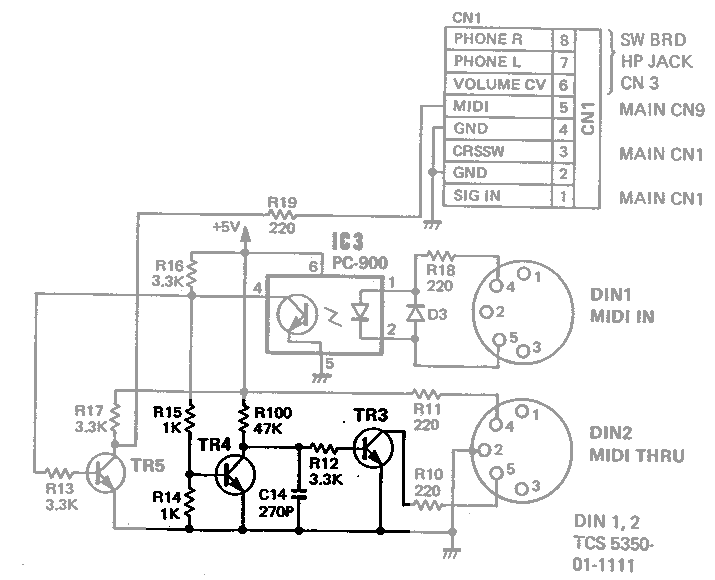
The capacitor, if it has been put there deliberately and does not just represent a parasitic capacitance, slows down switching on the second transistor. This might be useful if you want to balance the switching times (a saturated transistor is slower switching off than switching on). For example, such a capacitor is used in several Roland MIDI devices to ensure that the falling and raising edges of the MIDI signal are delayed by approximately the same amount:
Roland MKS-30 MIDI I/O

\$\endgroup\$

Your Answer

By clicking “Post Your Answer”, you agree to our terms of service and acknowledge you have read our privacy policy.

Not the answer you're looking for? Browse other questions tagged or ask your own question.