-1
\$\begingroup\$

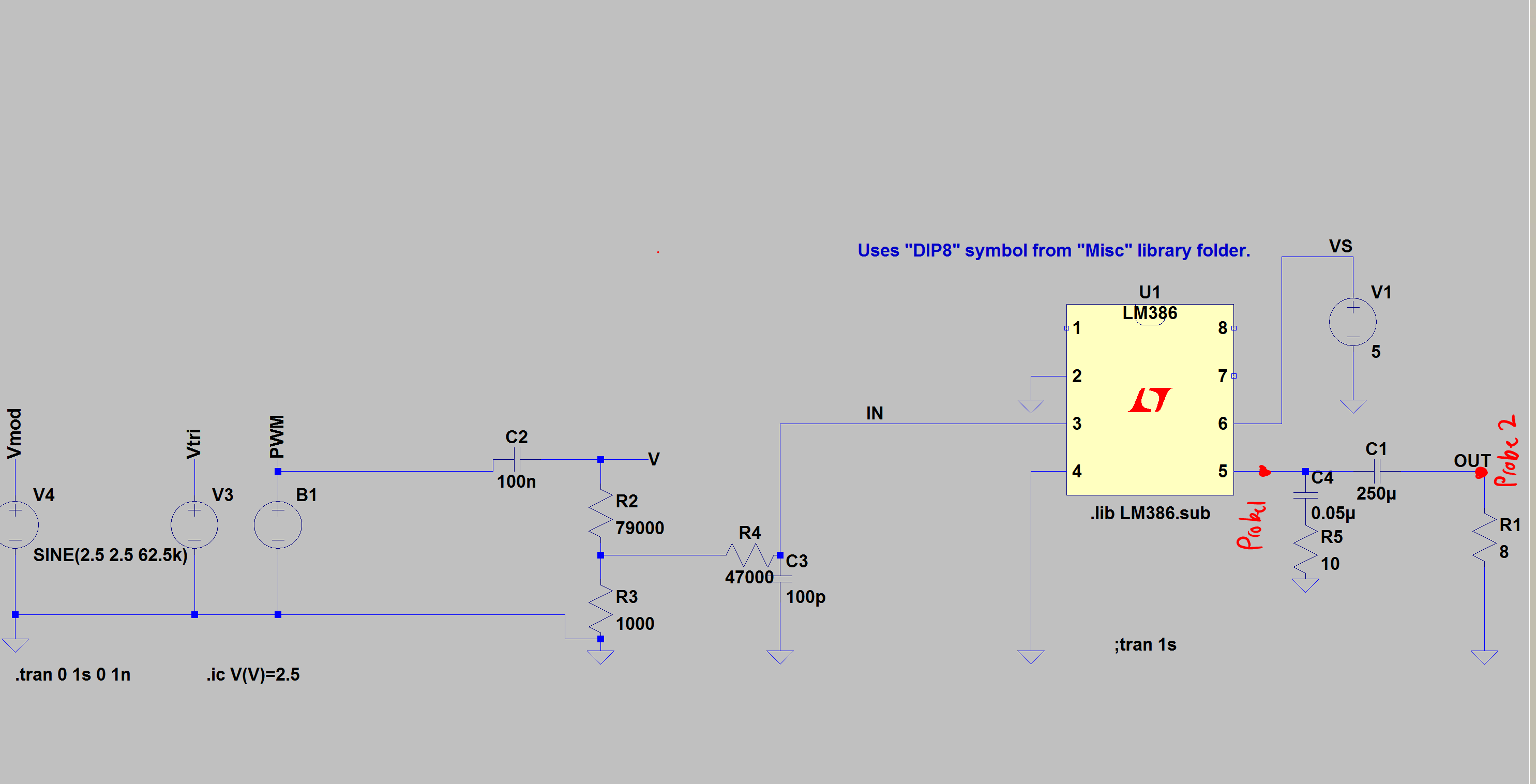
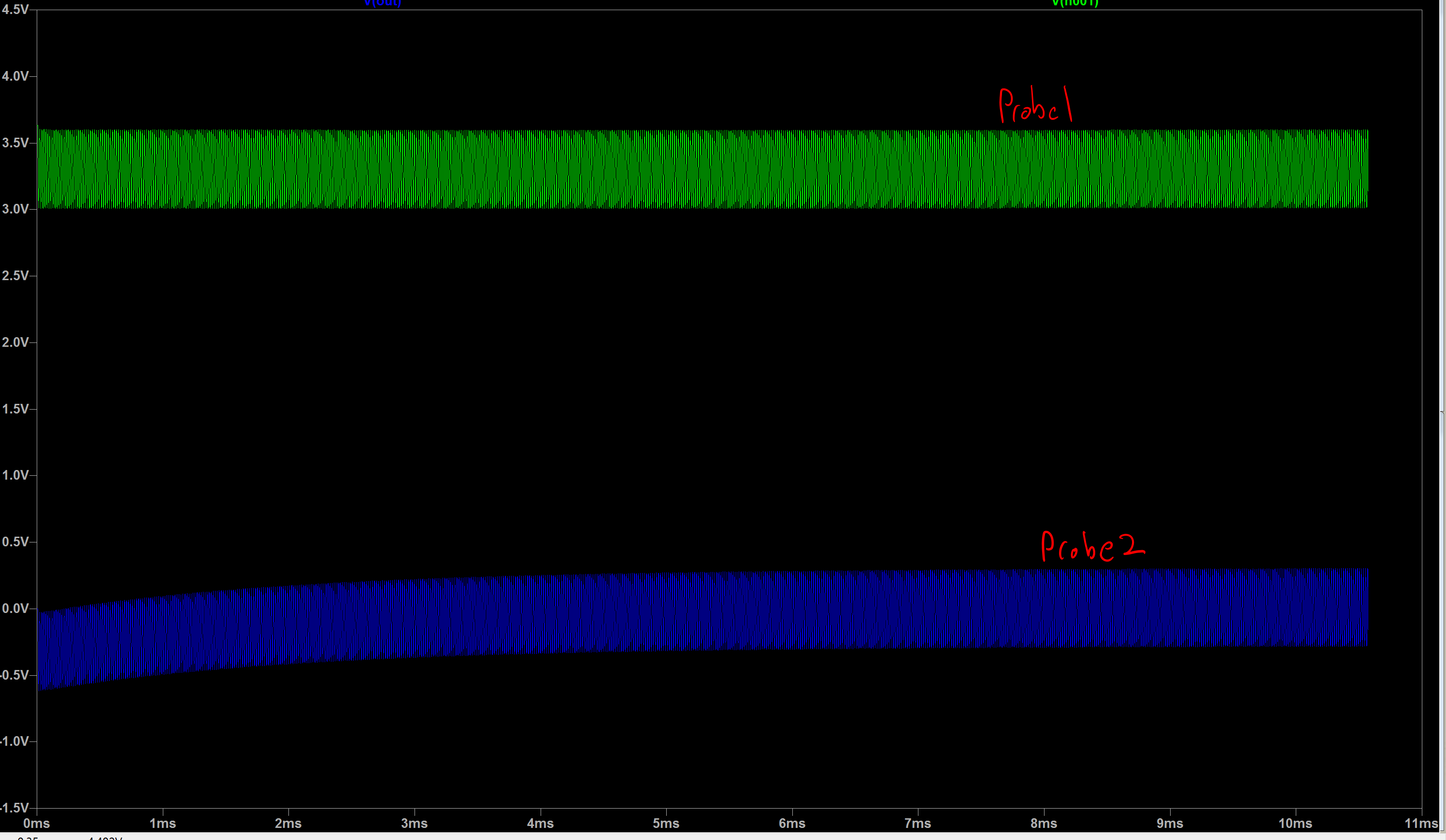
i am trying to create an analogue wave so that an audio signal can be played. Using PWM,(i.e. converting a square wave to an analogue signal hence need to use high pass then low pass filter before amp). For my circuit as shown below i have a high pass filter to remove the dc bias of 2.5V from my input source (5Vp-p, 2.5V dc bias, Amplitude=2.5V). I need the volatge divider after C1 so that my input voltage will drop to less than 0.4V to -0.4V. I have then used a low pass filter after this divider as i need to attenuate the frequencies of >30.5Khz (i understand >20kHz is not audible but it was stated that i should still use one, also converts signal to analogue type).

What i am having trouble with is:

  1. For my output wave (straight after my amp), the bias is at 3.3V but however i thought the output signal of the amp will give a dc bias of the VCC/2 so 2.5 in my case?

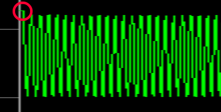
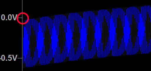
  2. For my final output signal going into the speaker (probed at the top node of the 8ohm resistor) my signal starts at a bias of around -0.3V but then levels out to a bias of around 0V. I am confused to as why the wave just doesnt start at 0V but instead levels out as seen. I understand this is only for 5ms then levels out but was just confused if it was posible to input a -ve wave into the speaker without a positive peak (i.e. usually ur inputting positive to negative waves)

For the components after the amp they have been placed there as they need to be there (i.e. remove dc offset of output wave for starters etc. Also are in the datasheet).

This circuit is what i have built and i was wondering if you could help explian why this output wave is looking like this.

Note: Please dont just say read the data sheet as i have looked at it many times or please dont just say this is the wrong circuit for this purpose as i believe that it is actually correct for my purpose. Also i know that my waves are pretty steep and arnt smooth essentially, as in i know i can use a higher order filter. Also i cant just actually test this in a real world application, such as by using an oscilloscope as i dont have the resources just yet available to me.

DATASHEET:http://www.ti.com/lit/ds/symlink/lm386.pdf

enter image description here

enter image description here

\$\endgroup\$
7
  • \$\begingroup\$ Your diagram has the input DC coupled. This is most likely not helping things. Did you delete another question about the 386 this morning? I could swear I saw that same diagram in another question. \$\endgroup\$
    – JRE
    Commented May 17, 2017 at 9:43
  • \$\begingroup\$ Sorry for some reason the wrong circuit was uploaded \$\endgroup\$
    – Student
    Commented May 17, 2017 at 9:55
  • \$\begingroup\$ You are STILL providing a DC path to ground from the opamp input. Do as the datasheet examples do instead. The LM386 looks after its own input biasing; you are upsetting that. \$\endgroup\$
    – user16324
    Commented May 17, 2017 at 10:17
  • \$\begingroup\$ So you are saying to not include the initial high pass capacitor for the input? Then how am I meant to drop the bias to 2.5 v to 0 v \$\endgroup\$
    – Student
    Commented May 17, 2017 at 10:23
  • \$\begingroup\$ AC couple the output of the voltage divider to the 386. Just a big capacitor in line to pin 3. \$\endgroup\$
    – JRE
    Commented May 17, 2017 at 11:17

2 Answers 2

1
\$\begingroup\$

my signal starts at a bias of around -0.3V but then levels out to a bias of around 0V. I am confused to as why the wave just doesnt start at 0V but instead levels out as seen.

Look closer. The output does start at 0V, but goes negative when the first cycle starts. The capacitor then slowly charges until the negative bias in the signal is removed.

enter image description here

enter image description here

But why does the signal start at the positive peak of the waveform, rather than in the middle? Perhaps because the LM386 blocked the signal for a short time when powered up, or perhaps the PWM wave is starting at the positive peak. A circuit with capacitors in it will require some time for them to charge up to stable DC voltages.

\$\endgroup\$
1
\$\begingroup\$

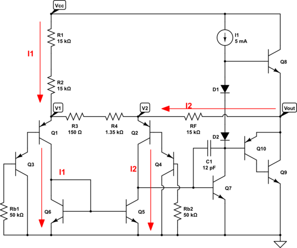
AD1 The voltage at the LM386 output will never be exactly equal to \$\frac{V_{CC}}{2}\$.

schematic

simulate this circuit – Schematic created using CircuitLab

Without input signal the voltage at \$Q_1\$ and \$Q_2\$ emitters is equal to:

$$V_1 = V_2 \approx 2V_{BE} $$

And the \$ R_1 R_2 \$ current is:

$$ I_1 = \frac{V_{CC} - V_{BE1} - V_{BE3}}{ R_1+R_2}$$

And since \$V_1 = V_2\$ no current will flow through \$R_3 R_4\$.

Hence, due to current mirror (\$Q_6, Q_5\$) action this \$I_1\$ current must be equal to: $$I_2 = \frac{V_{OUT} - V_{BE2} - V_{BE4}}{R_F}$$

$$I_1=I_2$$

$$\frac{V_{CC} - V_{BE1} - V_{BE3}}{ R_1+R_2}=\frac{V_{OUT} - V_{BE2} - V_{BE4}}{R_F}$$

And since \$R_1=R2=R_F\$ and \$V_{BE1}=V_{BE3}=V_{BE2}=V_{BE4}\$ we have:

$$V_{OUT} = \frac{V_{CC}}{2} + V_{BE}$$

AD2 - Do not worry about this. This is a transient state, \$C_1\$ capacitor need some time to be able to charge up at power-up. \$ T = 5*RC = 250\mu F*8 \Omega = 10ms\$.

\$\endgroup\$

Your Answer

By clicking “Post Your Answer”, you agree to our terms of service and acknowledge you have read our privacy policy.

Not the answer you're looking for? Browse other questions tagged or ask your own question.