I'm building a small watering control for one of my large indoor plants.
This is my first real electronics project outside of school. Although I studied EE at university and did my basic component and filter theory; I studied almost exclusively digital electronics. So PCB design and mixed signal circuits are all new to me.
Specs:
- Can drive 12V water pump up to 5A,
- Has level sensor in the water reservoir to prevent dry running the pump.
- Can read soil moisture from the pot.
- Can read soil temperature from the pot.
- Will automatically and instantly stop the pump if the pot overflows with water.
- Single power connector.
- Extensible.
- Easily programmable.
- UART for data retrieval.
The moisture is measured using a resistive voltage divider where the soil is seen as a resistors. The temperature is measured using a thermistor. And the overflow will be detected by large electrodes in the catchment tray under the pot if water ever makes it's way there, they will short out.
The pump will be driven by a 5V relay with 125R coil resistance (40mA, 200mW). The water level sensor will be a floating ring that will actuate a microswitch when the level becomes too low. The microswitch is NO and shorts to ground when closed. The internal pullup of INT1 pin will keep the signal high when the switch is open. The IRQ handler for INT1 will do debouncing.
I have two main connectors, P2 which goes to the pot and houses the overflow, temperature and moisture probes, and P1 which goes to the pump and has the water level sensor.
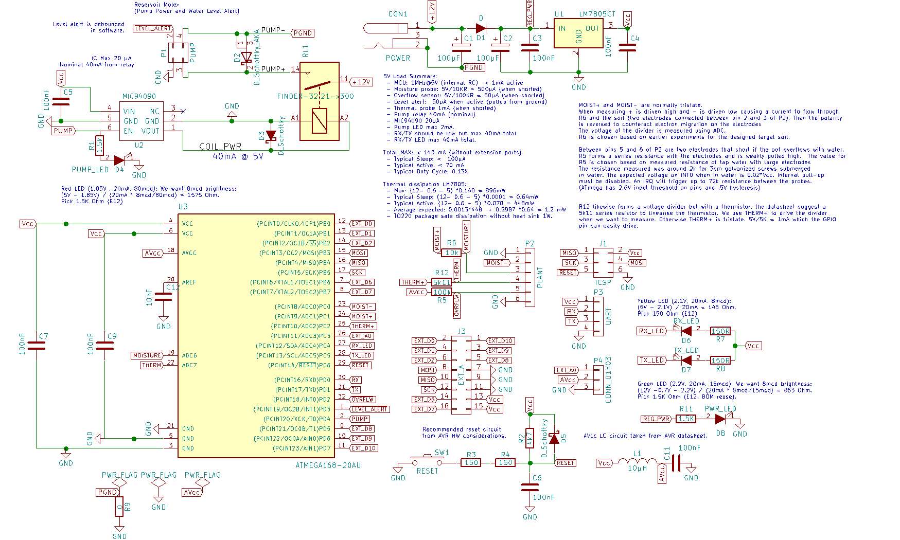
Circuit schematic:
I'm not sure about the resistor values for the LEDs yet, they're calculated for max brightness from the data sheets but I might go dimmer depending on how bright that is. I really have no idea. I'll adjust that when I have everything in my hand.
I attempted an estimate of the power drain from the regulator and I should be well within the tolerances for not needing a heat sink even at maximal draw. However typically the micro will probe the soil and if it is too dry (every 4-5 days) it will water it. Then it will go back into sleep mode for 4 hours. So the on-time is really short, around 20 seconds when it actually runs the pump compared to 4 hours sleep.
The MIC94090 (datasheet) is a high side load switch with 1.2A max continuous current. Do I need the freewheeling diode with this IC?
Should I add a small cap from LEVEL_ALERT to GND? I'm unsure about D2, do I need it? Is it harmful?
C1 is added because I'm concerned about the voltage dropping when the pump activates. I'm not sure how to calculate the drop, or if it is even a thing so I would appreciate some guidance on this. D1 is an isolation diode to try to prevent the voltage drop (if there is one) from dropping out the regulator.
I recon the internal RC oscillator divided down to 1 MHz will be sufficient for my application. 10 minutes this way or that way won't kill the plant.
The micro will be running a PID to control the duration of the pump based on how often it has to water. It will also do some low frequency data logging to EEPROM which can be read from UART. I'll do the math to make sure I don't exceed the write cycles in my lifetime.
I have not yet sourced all components or decided on which pump I'm going to use.
PCB layout
I will lay this out on a 2 sided PCB with 1oz/ft copper layer (35µm). I'm targetting seeedstudio to produce my PCB so I'm using a 6/6 rule and I will pay for 0.12mm solder mask.
I'm concerned about soldering the µC by the looks of it, even a 0.12mm solder mask will have hardly no mask between the pads. Will this be a problem?
I found so much different information on how to layout a mixed signal PCB, star ground, ground plane, split ground plane and truth be told I'm still not sure which way is the best. Based on the documents I found I went with a solid ground plane and keep routing of analogue signals and digital signals separated. Is this the preferred approach?
Although analogue performance is important, speed is not so I can to long sampling times to combat noise. I'm also using a "low noise mode" on the ATmega where I put the micro into power save mode during the ADC conversion which basically stops everything except the ADC clock and timer 2 which is my "wall" clock. So analogue and digital signals are by software mutually exclusive.
I tried my best to avoid current loops but I have to say I'm not entirely sure how to "see" the current loops and what constitutes a "patch antenna" which I've seen mentioned several times.
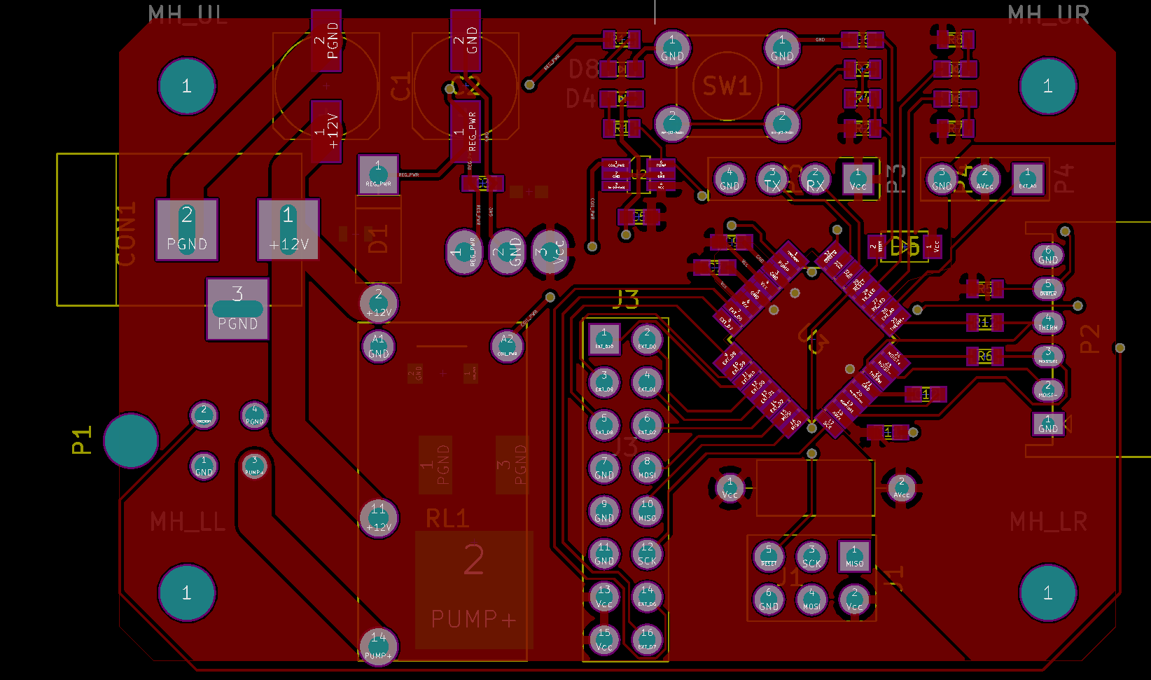
The board has 3 sections, to the left is "high power", the relay and pump connector possibly drawing up to 5A with an inductive load. The middle is 5V power and digital and the right is side is analogue. Note that digital wires are on the analogue side but they are by software quiet when the ADC is measuring.
The PCB will be put in a 3D printed case and fixed to the side of the planter box so that P2 (with the probes going into the soil) is facing up and P1 (pump and water level) is facing down.
Frontside PCB
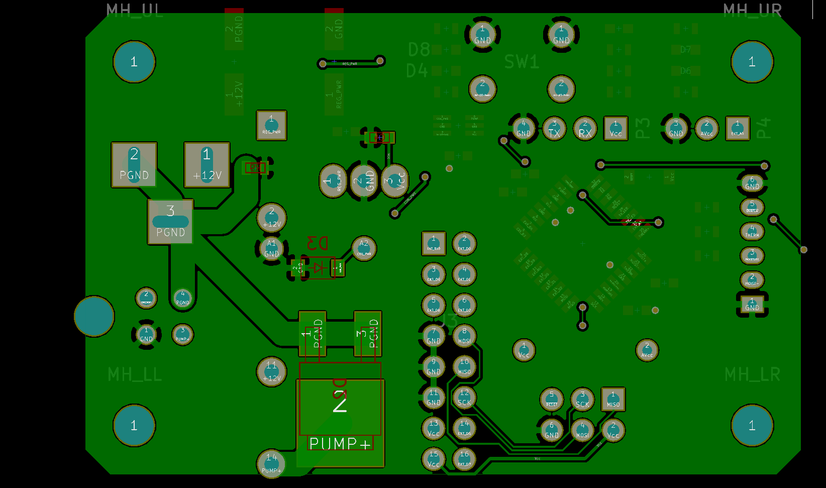
Backside PCB
I'm concerned about the routing of the ~LEVEL_ALERT signal, I couldn't manage a layout where the I could ever get a decent routing for it. I'm also concerned if the possibly large current in wires 3 and 4 of P1 may induce a current in the ~LEVEL_ALERT wire running parallel to them, which wrongly causes the µC to stop the pump.
I've tried my best to do a decent job at both schematic design and layout. Do you guys believe that this will work as intended?


