2
\$\begingroup\$

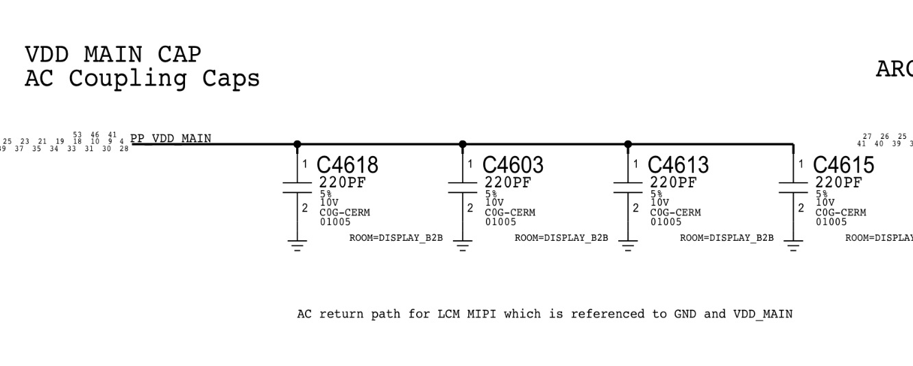
This is part of an iPhone 7 schematic. The VDD line is the main voltage rail for the phone.

I noticed this AC coupling tied to the LCM (display ground) I'm not familiar with MIPI but assume it has to do with connecting an external monitor to view display on the iPhone.

My understanding is that AC coupling caps is to allow ac to pass but block DC so, how would there be any AC on the main VDD line for implanting AC coupling caps? And what's the purpose?

enter image description here

\$\endgroup\$
10
  • 2
    \$\begingroup\$ @user140123 whoever sold you that schematic might have a different idea about nondisclosure than apple has. You certainly do. \$\endgroup\$ Commented Aug 1, 2017 at 20:03
  • 4
    \$\begingroup\$ The originality of this schematic excerpt isn't sufficient to account for any intellectually property rights. Nondisclosure doesn't apply if you don't have a contract (it's a problem of other people.) \$\endgroup\$
    – Janka
    Commented Aug 1, 2017 at 20:44
  • 1
    \$\begingroup\$ Agreeing with Janka! It's just that certainly apple wouldn't wish for their schematics to get disseminated, even in small portions (they have been very defensive about that in the past). I'm surprised a probably very professionally created and reviewed circuit does things like "PF" instead of "pF"; shows that even high-end tools probably still don't allow engineers to do exactly as they like. \$\endgroup\$ Commented Aug 1, 2017 at 21:52
  • 1
    \$\begingroup\$ @user140123 it's far from uncommon that development schematics and partner/user schematics are two different things. I've seen folks like guitar amplifier producers release schematics that willfully are wrong in the signal path, but hopefully helpful for fault finding, so that their devices are serviceable with those schematics. Honestly, these attempts were... funny at times (sure, yeah, let's have a weak resistor completely out of place in the negative feedback path of that tube...) \$\endgroup\$ Commented Aug 1, 2017 at 22:08
  • 3
    \$\begingroup\$ @user140123 don't underestimate the amount of communication and naming by convention that goes into such complex, team-developed schematics. Just because I don't understand how things are named doesn't imply it's not clever or helpful. I'm certainly no expert in hybrid signal schematic design, and frankly, I doubt you are, so I'd be careful with ridicule. \$\endgroup\$ Commented Aug 1, 2017 at 22:19

2 Answers 2

7
\$\begingroup\$

My guess:

The reason is explained on the schematic. It says "AC return path for LCD MIPI which is referenced to VDD_MAIN".

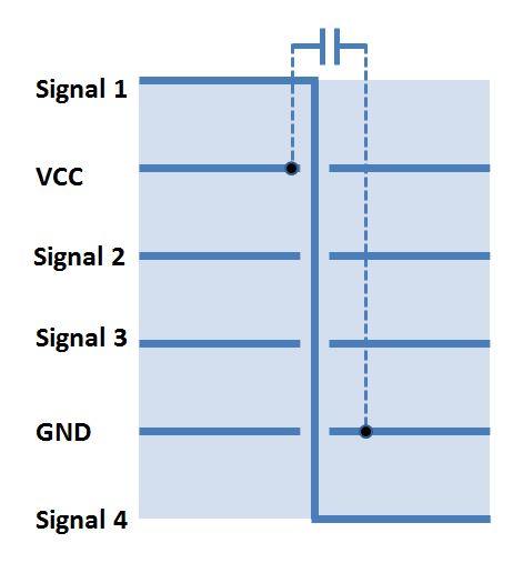
Most likely this means that some of the traces carrying fast MIPI signals use VDD as a reference plane. If these traces change reference planes to GND, for example through a via or a connector mating to a shielded flex, then caps between the two reference planes are required to allow the AC return current to find the shortest path and not wander around and cause EMI issues.

EDIT:

enter image description here

Say HF current flows into trace "Signal1". Return current will flow in the closest copper reference plane, here VCC. When the trace goes through a via, a stitching capacitor is added to allow the return current to also change layers. If both sides of the board had ground planes, a via would be enough.

\$\endgroup\$
5
  • \$\begingroup\$ Are MIPI signals in D.C. Current or AC? Or does it not matter the caps are merely to dissipate any AC that might occur on the line? \$\endgroup\$
    – user140123
    Commented Aug 1, 2017 at 22:14
  • \$\begingroup\$ You don't want spiky, high-frequency noise having to find its way to the bulk decoupling caps. You want a low resistance, low inductance path to high-frequency bypass caps as close as possible to the noise source. \$\endgroup\$ Commented Aug 2, 2017 at 0:05
  • \$\begingroup\$ see new edit... \$\endgroup\$
    – bobflux
    Commented Aug 2, 2017 at 8:47
  • \$\begingroup\$ @peufeu Thanks that helps but I'm still stuck on one thing, where would any AC noise come from? The MIPI signals? \$\endgroup\$
    – user140123
    Commented Aug 2, 2017 at 11:24
  • \$\begingroup\$ Yeah MIPI is fast digital signals so high frequency AC. I believe it uses LVDS, so each differential pair carries its own return current. In this case the caps only handle the common mode return current. \$\endgroup\$
    – bobflux
    Commented Aug 2, 2017 at 12:19
5
\$\begingroup\$

This is all speculation, but that's a complicated high-speed digital bus, and there's a lot of digital logic on the other end: Somehow, AC noise will couple onto VDD, be it in the cable or at the display end of things, and that noise is best gotten shorted to ground as early as possible, especially before it reaches other subsystems through shared power rails.

\$\endgroup\$
1
  • \$\begingroup\$ So even though there's tons of decoupling caps on that rail to block ac, the addition of coupled caps to allow ac to go to ground is still needed as extra protection? I thought maybe it had to do with display information since it says referenced to ground using MIPI? \$\endgroup\$
    – user140123
    Commented Aug 1, 2017 at 20:17

Your Answer

By clicking “Post Your Answer”, you agree to our terms of service and acknowledge you have read our privacy policy.

Not the answer you're looking for? Browse other questions tagged or ask your own question.