3
\$\begingroup\$

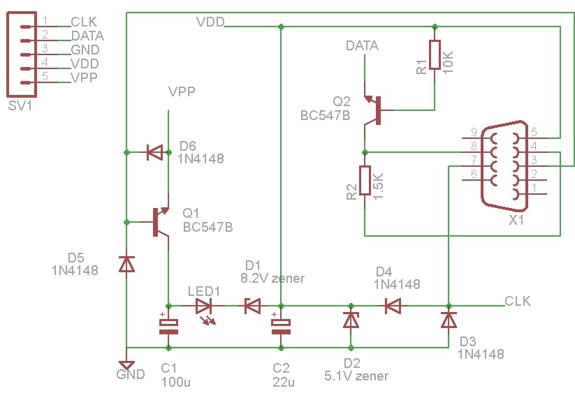
I am trying to build a JDM programmer for PIC. I looked at many circuit diagrams. During my analysis one thing I noted is that on most of the circuit diagrams the Vdd of PIC is connected to the GND of the serial port (pin 5). Can anyone clarify why it's connected like this?

enter image description here

This circuit is taken from: Puran's Blog - [DIY]+[PIC Programmer]+[IC-Prog].

\$\endgroup\$
1
  • 2
    \$\begingroup\$ @Sparky256 OP clearly states where he sees it: pin 5 of the serial port (X1 in the circuit) is directly connected to a net which the schematic labels as Vdd. If you read the linked article, there is a diagram showing pin 5 of that serial port to be GND. Unless I am missing something, OP is asking a very valid question - and I for one do not have the answer. \$\endgroup\$
    – InBedded16
    Commented Jan 30 at 17:44

1 Answer 1

7
\$\begingroup\$

The JDM PIC programmer by Jens D. Madsen is a "high voltage serial programmer" or HVPP. It is basically same as Ludipipo, Ludi's Pic Programmer, by Ludwig Catta.

It is intended to have a socket where you place the MCU to be programmed, it is not intended for having external connections for programming MCUs on PCBs, at least unless the PCB power supply is floating in respect to the PC so they don't share a ground.

The programmer uses the PC RS232 port which typically at the time used +/- 12V signaling for the data and handshake wires.

The PC GND is used as a positive MCU supply, as the RTS pin is set to negative to charge up C2 so the zener limits the MCU positive supply to about 5V. RTS will be clamped to about -6V by zener and diode. Toggling RTS between +/- 12V will pump up voltage to C1 which is the programming voltage reservoir cap, which will be limited to about 8V above MCU positive supply, or about 13V above MCU ground.

So the voltages are all relative. PC 0V is used as MCU positive 5.1V supply, to use PC negative -12V output as MCU 0V supply, which allows the PC positive +12V output to be used as the high voltage programming supply, about 13V above MCU 0V.

As the RS232 serial port outputs are not really intended to supply much power, the arrangement makes sure that the voltages are within the PIC requirements when load is applied and current is drawn from PC serial port data pins. The PC +12V will drop somewhat under load and which is why only +8V above PC 0V is needed because PC -12V is used to generate -5.1V as MCU ground.

\$\endgroup\$
4
  • 2
    \$\begingroup\$ I up voted your detailed and correct answer. \$\endgroup\$
    – Sparky256
    Commented Jan 30 at 20:10
  • \$\begingroup\$ @Justme Look like the capacitor C3 is typo. You mean C2? \$\endgroup\$
    – shafeeq
    Commented Jan 31 at 8:03
  • \$\begingroup\$ @shafeeq Yes I had off-by one typos, fixed. \$\endgroup\$
    – Justme
    Commented Jan 31 at 8:08
  • \$\begingroup\$ @Justme, Let me try to understand the working of the circuit. The C2, D2, D3 and D4 forms the power supply for the microcontroller. ie. the varying voltage between +15v and -15v in the RTS (pin 7) of RS232 will be rectified by D3 and D4, the C2 will be act as a filter capacitor and zener diode as a voltage regulator. Is my understanding correct? Could you add the use of other components to your answer? \$\endgroup\$
    – shafeeq
    Commented Feb 1 at 3:18

Your Answer

By clicking “Post Your Answer”, you agree to our terms of service and acknowledge you have read our privacy policy.

Not the answer you're looking for? Browse other questions tagged or ask your own question.