2
\$\begingroup\$

I am working on a hobby project to build a small audio amplifier. Actually the idea behind the circuit is to build a 0.5W-1W audio amplifier that can be powered from a single 9V battery and have decent audio performance in terms of THD. Keep in mind that I want it to be a discrete design and don't want to use any IC.

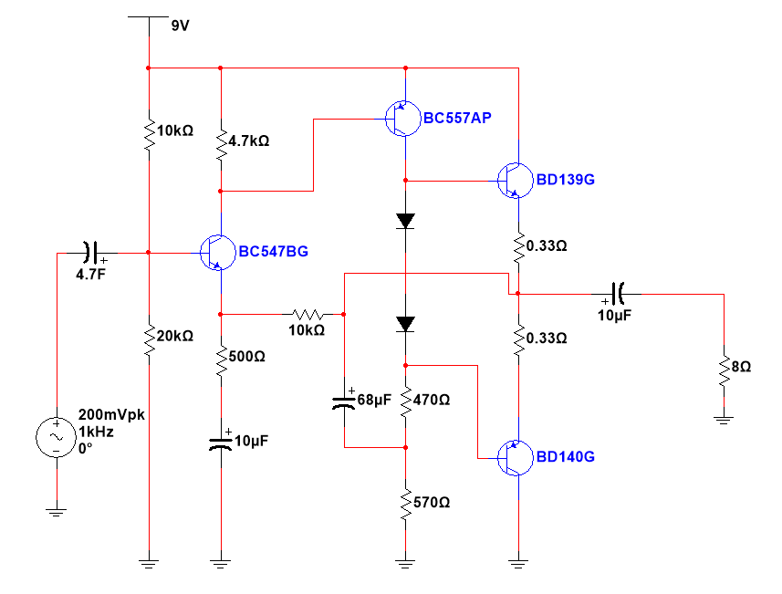
I have built and tested the following circuit with a pure sinusoid input 1KHz and a pure 8 ohm resistive load.

enter image description here Here is what I found

  1. The current in the driver stage (PNP) is between 6-7 mA. This seems to work best for 0.5W output. if reduced, the output distortion appears.

  2. The output signal swing is almost 6V pk-pk before it starts to show any signs of distortion. This means that I am getting 0.5W output.

  3. i have taken FFT of the output and tried to calculate THD with the above given working conditions, it is less than 1.5% at 1KHz. There are odd harmonics in the output at -60dB less than the fundamentamental freg.

  4. It sounds very clean.

Here is my question:

The output bias current with no input and no load is approx 12-13mA. As soon as I connect my input sinusoid and resistive load, it shoots up. For a maximum 6 V pk-pk swing it goes up to 120mA. If the output swing is reduced, the DC current also reduces. I don't understand this behaviour. Should not the DC current be constant and not affected by signal and load variation?

Please help me understand this. its killing me. I would like to know if the way im testing the circuit and measuring the DC current is correct and what would be a typical value of bias current for such a circuit?

Thank you all very much in advance for your feedback. Regards,VK

\$\endgroup\$
11
  • \$\begingroup\$ How are you measuring output bias current while the source and load are connected? \$\endgroup\$
    – Colin
    Commented Aug 16, 2017 at 9:19
  • \$\begingroup\$ Does the biasing current also increase for a much smaller input signal (like 10x smaller) ? I find the connections around the emitter of the input BC547 a bit strange, the emitter bias current can only pass through 10k to the ouput. This does not leave much headroom for this NPN. It could be that it saturates giving unexpected results. \$\endgroup\$ Commented Aug 16, 2017 at 9:24
  • \$\begingroup\$ Yes - the emitter circuitry for the BC547 looks VERY strange. \$\endgroup\$
    – LvW
    Commented Aug 16, 2017 at 9:40
  • \$\begingroup\$ @ Colin_s :I am meaasuring the current through the 0.33 ohm resistor. I connect the meter between the emitter terminal of BD139 and the 0.33 ohm resistor. \$\endgroup\$
    – user160109
    Commented Aug 16, 2017 at 10:00
  • \$\begingroup\$ @Bimpelrekkie: Yeah it does but like I said the increase in the biasing current is 'sort' of linearly related to the amplitude of the input signal. Hmm the DC voltages dont change much though. I have approx half supply voltage at the output. Maybe like you said BC547 is causing it. What I dont understand is why DC conditions change by changing the signal source which is isolated using a capacitor. \$\endgroup\$
    – user160109
    Commented Aug 16, 2017 at 10:05

4 Answers 4

2
\$\begingroup\$

The top transistor (BD139) supplies positive current to the load as well as bias current. It doesn't draw current FROM the load, only the bottom transistor does that - which is why it's called a push-pull amplifier.

You're only measuring the "push" half of the AC output waveform (in addition to the bias current) across that resistor, which, on a multimeter will look like a DC current.

So the increase you're seeing is NOT bias current but output current.

You can't eliminate it, other than by removing the load impedance or the AC input.

(Also, @Bimpelrekkie is right, there's an emitter resistor missing on the first stage)

EDIT : if you wish to measure the bias current separately from the output current, you'll have to measure the voltage across the 0.33R that is NOT currently supplying output - i.e. the lower one during positive half cycles, or the upper one during negative half cycles.

This pretty much requires a differential probe (or the difference between two channels) on an oscilloscope.

\$\endgroup\$
5
  • \$\begingroup\$ Thanks for your reply. I know that I'm measuring only push half of the signal. I have also measured the current through the lower 0.33 ohm resistor (or the pull side) and the values were close. \$\endgroup\$
    – user160109
    Commented Aug 16, 2017 at 12:40
  • \$\begingroup\$ That's the pull half. And your problem is... ? \$\endgroup\$
    – user16324
    Commented Aug 16, 2017 at 12:42
  • \$\begingroup\$ Hmm I think I'll check the way I'm measuring the current and post an update .. \$\endgroup\$
    – user160109
    Commented Aug 16, 2017 at 12:56
  • \$\begingroup\$ You were right about meter showing the push current as DC. It was my mistake thinking that it was the bias current only. Thanks for pointing that out!! \$\endgroup\$
    – user160109
    Commented Aug 18, 2017 at 10:24
  • \$\begingroup\$ About the resistor in the first stage. There is a DC path from the emitter to the output via 10K. The voltage across this resistor is about 1V which results in 100uA current. Maybe it's too small? but feedback fixes the problem like Bimpelrekkie mentioned. \$\endgroup\$
    – user160109
    Commented Aug 18, 2017 at 10:31
0
\$\begingroup\$

Power in = power out plus losses.

Power out is 0.56 watts (6 volts p-p and 8 ohm load)

Power in is 9 volts x 120 mA = 1.08 watts.

Losses are therefore 0.52 watts.

Sounds OK, not great but OK.

\$\endgroup\$
6
  • \$\begingroup\$ OK so why the down vote - the OP is measuring DC current (with a meter) and this increases as signal voltage increases for a given load. Should be fairly obvious but someone has down voted. \$\endgroup\$
    – Andy aka
    Commented Aug 16, 2017 at 10:36
  • \$\begingroup\$ It maybe obvious to you but I don't get it, that's why posted the question. You think I'd post a question if the answer was obvious to me? The answer you gave is not what I asked about. \$\endgroup\$
    – user160109
    Commented Aug 16, 2017 at 10:57
  • \$\begingroup\$ What meter are you using to measure the current through the 0.33 ohm resistor? What setting on the meter are you using? We are here to help and my knowledge of you is zero because, as it says on your profile "Apparently, this user prefers to keep an air of mystery about them". So, I answered assuming you had the meter set to DC and that would also show load current and my answer flowed down the route of you can't expect power out without power in and volts x amps is your power in..... \$\endgroup\$
    – Andy aka
    Commented Aug 16, 2017 at 11:01
  • 2
    \$\begingroup\$ So, before anyone goes downvoting an answer that they don't understand, have the courtesy of asking - I shouldn't have to question why someone has down voted my answer to get a response from you. Remember we are hear to help and not be abused. Down voting without explanation is abuse as far as I'm concerned. \$\endgroup\$
    – Andy aka
    Commented Aug 16, 2017 at 11:03
  • \$\begingroup\$ First I don't know who downvoted you because I did not. it's my first post here actually and I am still trying to find out how this works. My profile don't show much cause I just created it and the first thing in mind was to ask this question :) I have a degree in electronic engineering and analog electronics is my hobby. I learn something new everyday and I learn it by doing. Audio amplifiers (discrete designs) and switching voltage converters interest me. \$\endgroup\$
    – user160109
    Commented Aug 16, 2017 at 11:10
0
\$\begingroup\$

Hmmm Output bias current only has meaning when the output stage is in a quiescent state.It provides base current to the two complementary output transistors that sets a point on the V collector / I collector load line where it starts to become linear (normally curved for low base current).This curent is only constant when there is no input signal -When input is applied ( eg your 1khz test signal) this" bias point" actually moves with the signal, which obviously has to drive the base current beyond the no signal bias point ( signal generated base current essentially increases the bias current!!)- to yield power amplification. So bias current means exactly what it says - the output stage transistors are biased slightly on (ie BOTH conducting) when there is no input signal this is done to move the ouput load line into a linear portion of the V/ I curve.In perfect class B o/p stage, there would be no bias current at all.I dont see how you can measure "bias" when the ouput stage is amplifying a signal - it is meaningless as the static or standing DC bias at no input becomes an AC base driving signal when an ac input is applied. Bias current does need to be kept constant, it needsto decreases with the output device's temperature- Traditionally this was done using 2 emmiter base junctions of similar transistors to the ouput devices. These would be in place ofthe 2 diodes shown on your schematic, These 2 junctions voltage sepperate the 2 output device bases by approx 2 x Vbe. Furthermore the bias current needs to be reduced as the temperature of the Base collector junction of the ouput device rises. By placing the 2 emmiter base juctions in thermal contact with the output devices -some degree of thermal compenstaion can be achieved.

\$\endgroup\$
0
\$\begingroup\$

As said by the others, bias should be measured as voltage across the emitter resistors of the output stage without load and input signal (or else you will be measuring the output current of the amp).

OK, how to set the bias in a push-pull class-AB output stage...

The Vbe of your BD139 and BD140 depends on the transistor's internal junction temperature. It decreases by 2mV/°C.

At idle conditions, a decrease in Vbe will cause a higher current to pass through the transistor, which causes it to heat, which decreases Vbe, which increases current...

With only 9V on the supply, your transistors don't risk going into thermal runaway, but the diodes should be thermally coupled to the heatsink. This way, when the transistors heat, the diodes' voltage drop decreases by the same 2mV/°C, and this compensates Vbe change.

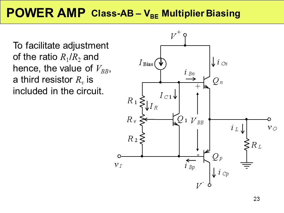
There is a better circuit through, which is used quite universally in power amps:

enter image description here

(image credit)

The circuit around Q1 creates a voltage between the two transistor bases. Q1 acts as a common emitter amplifier, which amplifies its own Vbe by a ratio set by the potentiometer. Q1 is installed on the power transistors heatsink, so it follows the output transistors' temperature and compensates for it.

Then you simply adjust the pot to get the bias current you want, while monitoring the voltage on the power transistors' emitter resistors (not shown on this schematic).

Just replace your two diodes with this Vbe-multiplier, attach the transistor to the heat sink, and set the bias with the pot, it's quite practical.

Now, about your circuit:

The output transistors are current-driven, thus crossover distortion behaviour will depend on how their hFe matches, and the value of emitter resistors is not critical.

The circuit around the input transistor is weird. Current in the BC547 is set by feedback, to make the voltage on the 4k7 resistor equal to Vbe of BC557. Thus the input transistor is biased at 130µA, which is very low. Across the 10k feedback resistor, this creates a 1.3V drop, this must be why the 10k/20k resistors which set the DC base voltage of BC547 are not equal...

\$\endgroup\$

Your Answer

By clicking “Post Your Answer”, you agree to our terms of service and acknowledge you have read our privacy policy.

Not the answer you're looking for? Browse other questions tagged or ask your own question.