4
\$\begingroup\$

I am reading "Advanced Thermal Management Solutions on PCBs for High Power Applications":

https://ats.net/wp-content/uploads/2014/04/Advanced-Thermal-Management-Solutions-on-PCBs-for-High-Power-Applications_APEX2014.pdf

And on page 4 is states that:

It can be seen that the thermal vias are situated in the extended thermal pads beside the pad, where the component will be placed. So, to avoid the well-known problem of solder soaking, it is not possible to place open thermal vias directly underneath a component.

I have never heard of "solder soaking", can someone please explain what the author means?

EDIT:

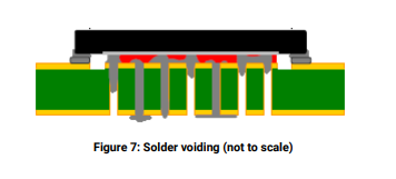
I found something called "Solder voiding" in another document which seems to be the same thing:

enter image description here

\$\endgroup\$
7
  • \$\begingroup\$ Not sure if I would call it soaking, but guess what happens with solder on an open via when it melts... \$\endgroup\$
    – PlasmaHH
    Commented Nov 22, 2017 at 10:44
  • 2
    \$\begingroup\$ @Time Mottram This is probably the wrong link? I don't know if this is the correct term they used but what they meant is probably that such open thermal vias will drain the solder from your thermal pads. \$\endgroup\$
    – Manu3l0us
    Commented Nov 22, 2017 at 10:47
  • \$\begingroup\$ Yep, sorry, fixed it. \$\endgroup\$
    – Tim M
    Commented Nov 22, 2017 at 10:50
  • \$\begingroup\$ Yeah, that's what I thought but I was wondering if anyone with more knowledge than me knew, it says "well-known"... \$\endgroup\$
    – Tim M
    Commented Nov 22, 2017 at 10:52
  • 2
    \$\begingroup\$ The voiding is the lack solder (marked red in this image) created in this case due to solder wicking (solder flowing down the vias) \$\endgroup\$
    – Manu3l0us
    Commented Nov 22, 2017 at 11:26

1 Answer 1

1
\$\begingroup\$

It has been mentioned in the comment by Manu But I'll elaborate here in an answer:

When placing thermal vias underneath a component with a thermal tab and these vias are open, then the solder will suck through the vias because of capillarity. When this happens, it can happen that's there's not enough solder left in order to make a reliable bond. The result is that the thermal enhancement effort makes things worse.

The solution is to close the vias through plugging, e.g. with silk screen (=tenting, not recommended as there are no guarantees) or dedicated plugging.

\$\endgroup\$
4
  • \$\begingroup\$ I'm not sure that you would ever want to plug a via with silk screen, especially under a thermal pad. \$\endgroup\$ Commented Mar 3, 2018 at 14:54
  • \$\begingroup\$ I agree, it's a poor man's solution to real plugging. Edited. \$\endgroup\$
    – gommer
    Commented Mar 3, 2018 at 14:59
  • 2
    \$\begingroup\$ I think they call the practice "tented vias" its an option on PCB design software like Altium. I agree with it being a bad plan. \$\endgroup\$
    – Tim M
    Commented Mar 8, 2018 at 14:23
  • \$\begingroup\$ Indeed, tenting it is. Edited. \$\endgroup\$
    – gommer
    Commented Mar 8, 2018 at 15:16

Your Answer

By clicking “Post Your Answer”, you agree to our terms of service and acknowledge you have read our privacy policy.

Not the answer you're looking for? Browse other questions tagged or ask your own question.