1
\$\begingroup\$

Is there a surface-mount component I can put on a pad, that simply has another pad on top that I can solder something on to?

Here is a side view showing pins above the pads that would need bent down to contact the pads: End-mounted TO Can Side View
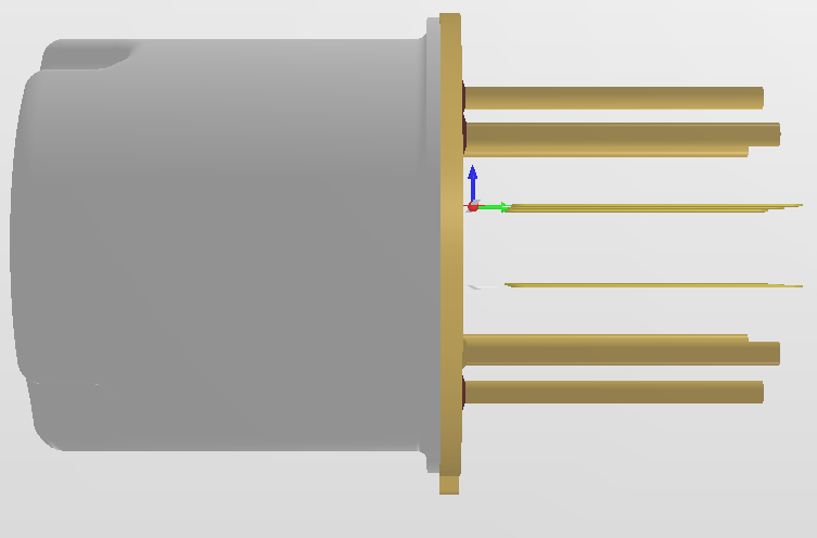
Here is a top view to show how the pins align with the pads: End-mounted TO CAN Side View
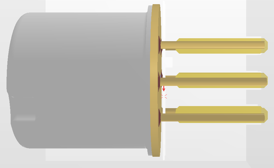
We found that edge-mounting a TO-Can package to a PCB will really save a lot on manufacturing. However, it comes with fairly long through-hole pins that are taking up too much space. We could trim the pins, but then we cant bend them enough to reach the pads on our 0.062" PCB. We can't make the PCB thicker because we're also end-mounting a connector that constrains the PCB thickness.

Someone here had the idea of using high-resistance SMD resistors. That could work but it seems like you wouldn't get much soldering area on top.

Mechanical strength should not be an issue since the whole assembly will be overmolded and encased in plastic.

I looked through what seemed like hundreds of right-angle receptacles, etc. to do the job, but couldn't find anything.

It needs to raise it 1.5-2mm above the PCB surface.

Any suggestions or solutions would be appreciated!

\$\endgroup\$
8
  • 1
    \$\begingroup\$ When you say "end-mounting" I think you mean to say "edge-mounting" which would make your post a lot more clear. I hope you save a lot of money during assembly because all the methods I can think of are labour intensive. It's also not entirely clear how this is suppose to work since your component has 6 pins sitting at 4 different heights above or below the PCB. Do you not care about all the pins? \$\endgroup\$
    – DKNguyen
    Commented Apr 24, 2021 at 0:49
  • 1
    \$\begingroup\$ Why can’t you get the proper part in SMT? \$\endgroup\$
    – D.A.S.
    Commented Apr 24, 2021 at 0:54
  • 1
    \$\begingroup\$ You can buy contact pads. They are not designed specifically for what you are doing, and they are less than 1.5mm. Example mouser.com/pdfdocs/harwinsmtcontactpadsdatasheet.pdf \$\endgroup\$
    – user57037
    Commented Apr 24, 2021 at 17:31
  • 1
    \$\begingroup\$ Also, 1.6 mm is a common PCB thickness. Maybe you can just use a small PCB as a "lifter". \$\endgroup\$
    – user57037
    Commented Apr 24, 2021 at 17:33
  • 1
    \$\begingroup\$ @mkeith if some offset is allowed then maybe thicker support PCB would be better, to be used on one side only, the other is soldered directly to main board. Unfortunately middle pins would still need bending \$\endgroup\$
    – Maple
    Commented Apr 25, 2021 at 7:20

3 Answers 3

2
\$\begingroup\$

it seems like you wouldn't get much soldering area on top

2 mm thick SMD resistors are quite large, there should be enough soldering area.

I don't get why you think of "high-resistance" parts though. In fact, you need 0 Ohm jumpers. Put 6 of them along the leads and you would have two points of solder contact for each lead. Also jumpers often have metallized ends larger than normal resistors in same package size.

You can even use SMD capacitors or inductors this way, whatever is cheaper and has suitable dimensions.

An added benefit is that you can find SMD parts with exact height for each lead and have them installed by the machine. Then manual labor step will be quick and easy.

\$\endgroup\$
3
  • \$\begingroup\$ I didn't think of placing them along the pads, that is a great idea. Then you get a nice support for the pin, and the pick and place machine can have them there ready. That gives us a lot of flexibility to match heights and lengths. \$\endgroup\$
    – Luminaire
    Commented Apr 24, 2021 at 17:03
  • \$\begingroup\$ One other advantage of this solution is it allows me to recover the board space taken up by the large pins without trimming them. I can position the SMD jumpers under the ends of the pins, and then have some free space underneath the pins, between the jumpers and the board edge. As long as I take care to only place components a good deal shorter than the SMD jumpers. But trimming the pins should be trivial for manufacturing so I might still go that route \$\endgroup\$
    – Luminaire
    Commented Apr 24, 2021 at 17:27
  • 1
    \$\begingroup\$ @Luminaire yes, this should free some space for other components. One advice - when you select SMD parts for support try experimenting with heights and choose slightly taller (0.1~0.2mm) than you need. Then TO part will go with tight fit and will be easier to solder. Also the leads will press down on SMD and prevent them from moving when solder melts. \$\endgroup\$
    – Maple
    Commented Apr 24, 2021 at 21:17
3
\$\begingroup\$

I would consider making a small (eg. 9mm x 9mm) right-angle PCB and joining it by solder either on the edge or in a slot depending on how long the leads are. You could notch the board for more positive location on the edge.

\$\endgroup\$
8
  • 1
    \$\begingroup\$ A variant of this is custom FPC, that does not require tricky soldering. There were similar suggestions at the link in a question, for some reason disregarded by OP. \$\endgroup\$
    – Maple
    Commented Apr 24, 2021 at 5:05
  • 1
    \$\begingroup\$ @Maple I don’t think the soldering would be tricky at all, I laid it out schematically before posting this answer. It would, obviously, have to be done by hand and might require a simple jig. \$\endgroup\$ Commented Apr 24, 2021 at 5:28
  • 1
    \$\begingroup\$ @SpehroPefhany That is an excellent idea. I can see how it would work, your right angle PCB can have mating slots and pads that align with slots/pads on the main PCB, giving you a right angle pad to join together. We are already planning on making a jig for assembly so that is no problem. I think your solution would work great. I'm going to run this and the SMD jumpers by my team and see which one they think will work better \$\endgroup\$
    – Luminaire
    Commented Apr 24, 2021 at 17:16
  • \$\begingroup\$ @Maple you're right I had disregarded the custom FPC because the pins are not in straight lines, so a flat FPC with SMD pads would only contact 2 of the 3 pins on a side. But now it occurrs to me that the FPC can have through-hole connections just like a PCB. So that could actually work! \$\endgroup\$
    – Luminaire
    Commented Apr 24, 2021 at 17:22
  • 2
    \$\begingroup\$ @SpehroPefhany OP is also planning on overmolding. That probably removes any structural strength concerns once it is done. \$\endgroup\$
    – Maple
    Commented Apr 24, 2021 at 21:37
2
\$\begingroup\$

Try this:

https://www.elmisrl.it/wp-content/uploads/2017/03/080042A_Distanziatore_TO5-A0_1.jpg


Also look for "spacer for transistor TO-5"

\$\endgroup\$
5
  • 2
    \$\begingroup\$ Op is asking for edge mounting. The text is not as clear as it could be. \$\endgroup\$
    – DKNguyen
    Commented Apr 24, 2021 at 2:07
  • 1
    \$\begingroup\$ Link-only answers are discouraged. They're useless when the link dies. Why not embed the image in your answer? \$\endgroup\$
    – Transistor
    Commented Apr 24, 2021 at 17:01
  • \$\begingroup\$ @DKNguyen thanks your clarification is correct \$\endgroup\$
    – Luminaire
    Commented Apr 24, 2021 at 17:23
  • 1
    \$\begingroup\$ I'll substitute the link on Monday. \$\endgroup\$ Commented Apr 24, 2021 at 17:23
  • 1
    \$\begingroup\$ @enricomigliore Good to know to search for transistor TO-5, that is pulling up way more stuff than I was finding \$\endgroup\$
    – Luminaire
    Commented Apr 24, 2021 at 17:24

Your Answer

By clicking “Post Your Answer”, you agree to our terms of service and acknowledge you have read our privacy policy.

Not the answer you're looking for? Browse other questions tagged or ask your own question.